MOCVD-grown InP nanowires hit solar scene
The budding field of nanowire solar cells could be enhanced by making compound semiconductor devices using selective-area epitaxial techniques, Japanese researchers say.
A collaboration between Japanese conglomerate Honda and Hokkaido University has produced InP core-shell nanowires that it claims are individually 12.3 percent efficient in converting light to electricity.
The researchers used an MOCVD production technique that avoids the problem of catalyst contamination seen in the most popular nanowire production approach, the vapor-liquid-solid growth method. That contamination problem reduces the efficiencies of the resulting nanowires.
Consequently, in a paper published in Applied Physics Express on February 29, the team says the efficiency it records is “quite high for a prototype device”.
Junichi Motohisa, a professor in the Hokkaido University team, explained that core-shell nanowires cells could offer a better compromise of light absorption and carrier diffusion than planar cells.
Motohisa and his co-workers produced a prototype cell using p-type core InP nanowires with an average internal diameter of 135 nm, surrounded by n-type material that increased the overall nanowire diameter to 209 nm.
“We started the development of solar cells with InP because issues related to surface states, which are sources of carrier recombination loss, are less important than in GaAs,” he told compoundsemiconductor.net.
The key to growing nanowires rather than continuous layers is a patterned 20 nm thick silica film formed on top of the cell s InP substrate.
In this film the Honda and Hokkaido team formed 130 nm holes separated by 400 nm, using wet etching and electron-beam lithography. Motohisa says that nanoimprint lithography will be the most effective method for producing these patterns in large volumes.
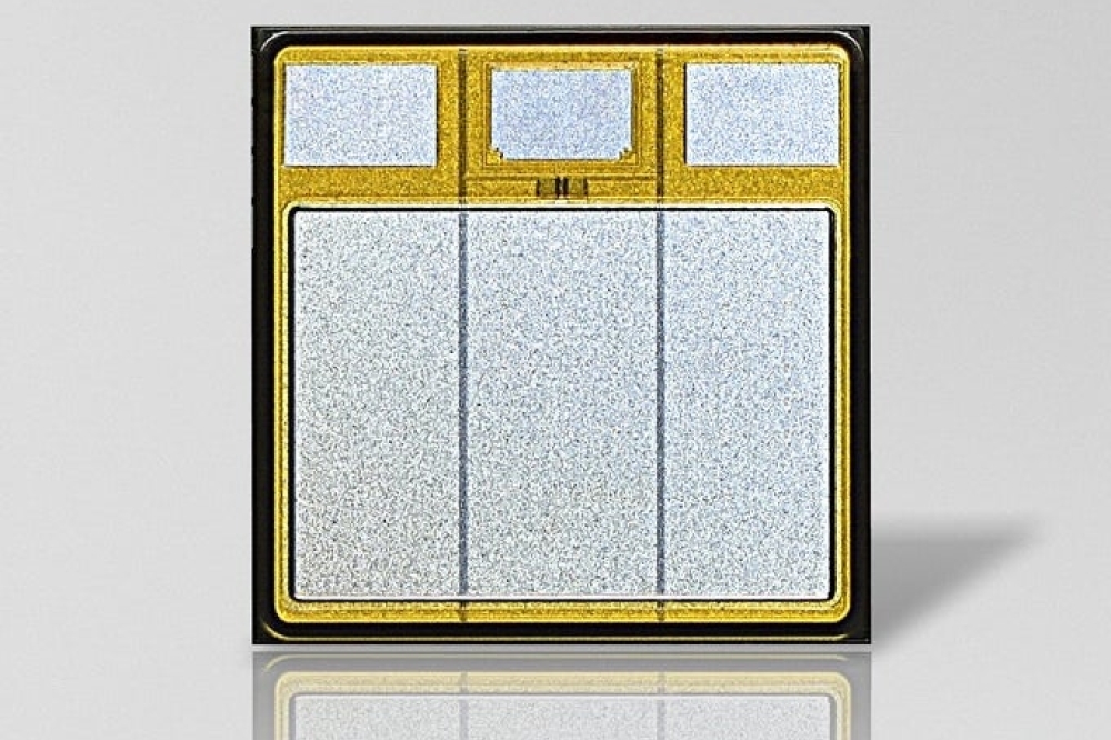
After depositing the nanowires they made a photovoltaic device by filling the space between the nanowires with resin, then attaching silver/indium tin oxide and gold-zinc alloy electrodes.
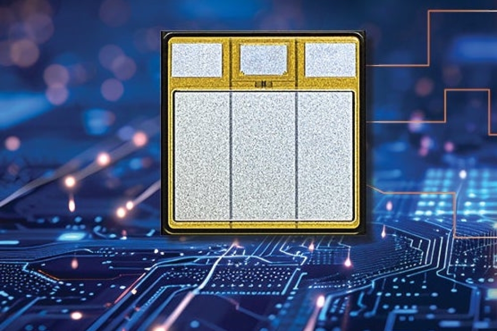
The final cell had three active 2.0 mm x 2.6 mm nanowire segments in its overall 1.0 cm x 1.0 cm surface area.
Under Air Mass 1.5 Global (AM1.5G) standard illumination the cell produced 0.43 V open circuit voltage, at 3.37 percent overall efficiency.
While nanowire cells are clearly some way from commercialization, Motohisa emphasized that Honda's interest was reflected by its existing solar manufacturing operations in Japan.
The Hokkaido academic anticipates that nanowire solar cells will not see their first use in terrestrial power generation. “Space application is the most straightforward as GaAs or InP planar solar cells are mainly developed for that purpose,” he said.
Nanowires improve sunlight absorption by effectively working as an antireflective coating, Motohisa points out. Also, because the whole active area's surface is not covered with nanowires such cells use less semiconductor material overall.
“If the issues of material and production cost could be overcome, their potential high conversion efficiency would open up a possibility for consumer products,” he said.


