News Article
RFMD adds low cost high power IPCs to portfolio
High Power Integrated Passive Component (IPC) Technology will enable foundry service customers to design integrated matching networks and other passive functions on low-cost GaAs process technology
RF Micro Devices announced it will begin providing IPC technology to customers of its Foundry Services business unit in June 2010.
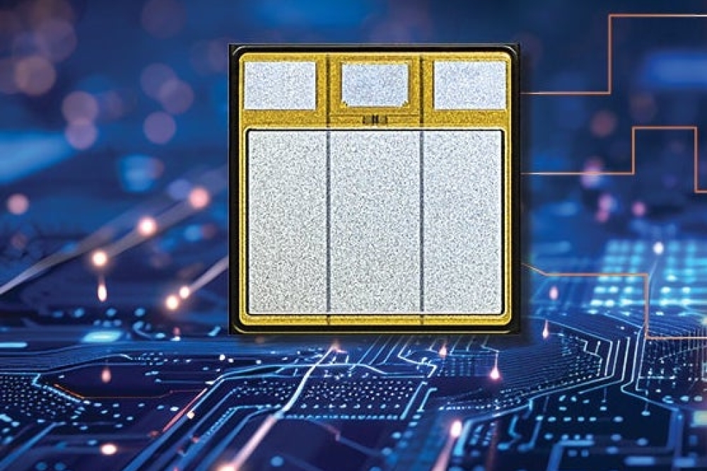
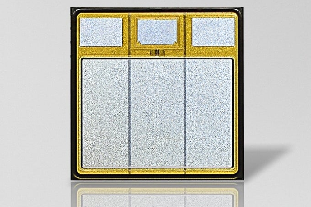
Complementary to its GaN technology and other power semiconductor technologies, the IPC is suited to the design of multi-chip modules (MCMs) and will reduce costs and achieve higher levels of integration by leveraging scale and cost structure in GaAs and GaN manufacturing.
RFMD's IPC technology provides all of the passive circuit components necessary to enable matching networks, including MIM capacitors, multi-layer stacked capacitors, thin-film resistors and inductors. Additionally, three metal interconnect layers are available for complex routing and increased current-handling capability.
Bob Van Buskirk, president of RFMD's Multi-Market Products Group (MPG), commented, "RFMD's leading compound semiconductor scale, built to serve the cellular handset market, allows us to deliver industry-leading cycle time, yields and costs. We enable our foundry customers to take advantage of a compound semiconductor factory capable of shipping over two million RF components per day to bring speed, predictability and price advantages difficult to match."
RFMD's GaN Foundry Services business unit currently offers foundry customers access to two GaN process technologies: GaN1, targeted at high power, and GaN2, targeted at high linearity applications.
RFMD's Foundry Services business unit was formed to supply RFMD's high-reliability, high-performance and price-competitive GaN processes and associated technologies to external foundry customers immediately upon process qualification and production release.
It offers a secure website to customers for use as a collaboration tool for their work with RFMD's GaN foundry. All necessary tools and documents are current and readily available, including:
-- Monthly schedule for multi-project wafer shuttle runs
-- Process design kits (ADS, AWR)
-- Design rule check and layout versus schematic runsets for layout verification using Calibre
-- Complete descriptions of the design rules
-- Step-by-step instructions for each stage of the foundry process
-- A private access folder for secured uploading and downloading of confidential files


