Laser and 10Gb/s Silicon Modulator Using CMOS Fabrication Processes
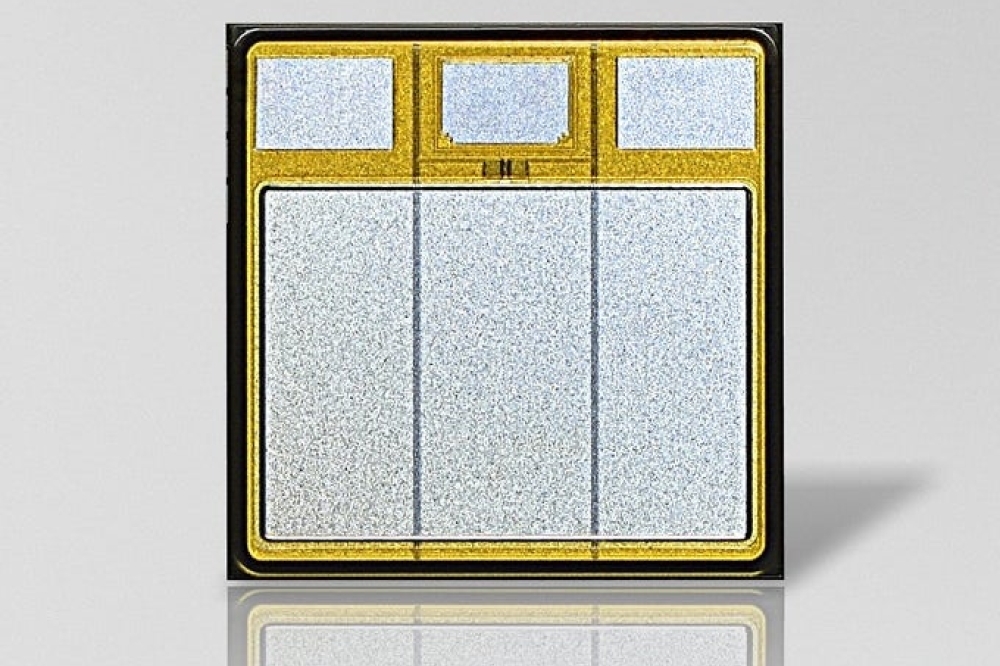
Silicon photonics is an emerging technology for overcoming electrical connections’ limits in processing increasingly data-rich content and reducing the cost of photonic systems by integrating optical and electronic functions on the same chip. The technology may enable low-cost solutions for a range of applications such as optical communications, chip-to-chip and rack-to-rack connections, data-center cables, optical signal processing, optical sensing, and biological applications. The project, in its second year, is developing building blocks and processes to accelerate the adoption of silicon photonics. The laser was fabricated by first bonding a III-V material (indium phosphide) on top of a CMOS wafer and then processing it using the same equipment as in microelectronics production. The project, in its second year, is developing building blocks and processes to accelerate the adoption of silicon photonics. The laser was fabricated by first bonding a III-V material (indium phosphide) on top of a CMOS wafer and then processing it using the same equipment as in microelectronics production. The consortium also demonstrated a 10Gb/s silicon modulator with an extinction ratio of 7dB. The 40Gb/s version has already been designed by the consortium and is under fabrication. First characterization results are expected next year. “The capability of manufacturing optical components within the CMOS-processing infrastructure is key to realizing the potential of silicon photonics,” said Laurent Fulbert, photonics programs manager at Leti and coordinator of HELIOS. “The HELIOS partners are focused on bringing this technology to foundries and component manufacturers for high-volume applications.” In addition to the laser and silicon modulator, building blocks under development by the HELIOS partners include a light modulator, passive waveguides and photodetectors. Other recent results of the project include: •Demonstration of high responsivity (0.8-1A/W), low dark current and high BW photodiodes (up to 130 GHz) •Efficient passive waveguides (Mux/Demux, polarization diversity circuit, fiber coupling, rib/strip transition) •Establishment of a photonics design flow •Investigation of novel concepts for light emission and modulation Most of the results of the second year have been presented at the IEEE Group Four Photonics Conference in Beijing. The HELIOS consortium also developed a training course addressing all aspects of silicon photonics. This free, 21-hour course is available on HELIOS website: http://www.helios-project.eu/Download/Silicon-photonics-course In addition to Leti, the HELIOS partners are: - imec (Belgium) - CNRS (France) - Alcatel Thales III-V lab (France) - University of Surrey (UK) - IMM (Italy) - University of Paris-Sud (France) - Technical University of Valencia (Spain) - University of Trento (Italy) - University of Barcelona (Spain) - 3S Photonics (France) - IHP (Germany) - Berlin University of Technology (Germany) - Thales (France) - DAS Photonics (Spain) - Austriamicrosystems AG (Austria) - Technical University of Vienna (Austria) - Phoenix BV (Netherlands) - Photline Technologies (France) The HELIOS Project website address is www.helios-project.eu/


