News Article
Measure and manipulate charged species in GaAs with STM
Scanning Tunnelling Microscopy (STM) can be used to position charged vacancies and adatoms on the surface of a semiconductor, suggesting a new and direct method for quantifying the charge of defects and adsorbates at surfacs.
The scaling of transistors to nanometre dimensions requires more precise control of individual dopants in semiconductor nanostructures. This is because statistical fluctuations in dopant distributions can significantly impact device performance.
Proposals for next-generation quantum- and spin-based electronics also rely on the tuning of the charge, spin and interactions of dopant atoms with local electric fields.
Using a scanning tunnelling microscope (STM), researchers at Ohio State University have demonstrated how to control the binding energy and ionization state of individual acceptors in p-doped GaAs .
Charged species such as native dopants, vacancies and adatoms directly influence the acceptor binding energy via the Coulomb interaction. In addition, a combination of defect- and tip-induced band bending can be used to remotely tune the acceptors' ionization state.

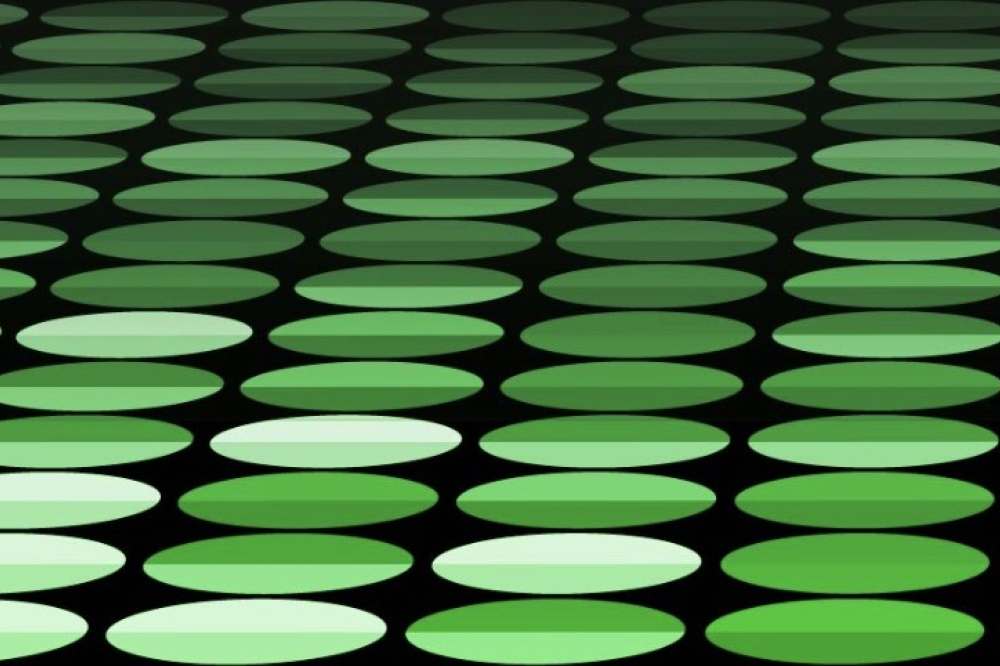
This microscopic image of the surface of gallium arsenide (GaAs) shows how the arrangement of atoms on the GaAs surface affects its electric field. The image illustrates the manipulation of individual atoms to allow for very precise tuning of the characteristics of GaAs-based transistors.
The scientists found that by applying voltage pulses with the STM tip, charged vacancies and adatoms can be positioned on the surface. These experiments suggest a new and direct method for quantifying the charge of adsorbates (e.g. adatoms or molecules) as well as defects (e.g. vacancies, antisites, interstitials) at semiconductor surfaces.
Further details of this work will be presented by Jay Gupta in the talk “STM manipulation and measurement of charged species in semiconductors” at the APS March Meeting 2011 in Dallas, Texas on Monday, March 21, 2011between 9:12am - 9:48am.


