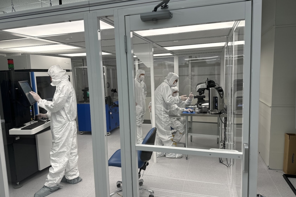
News Article
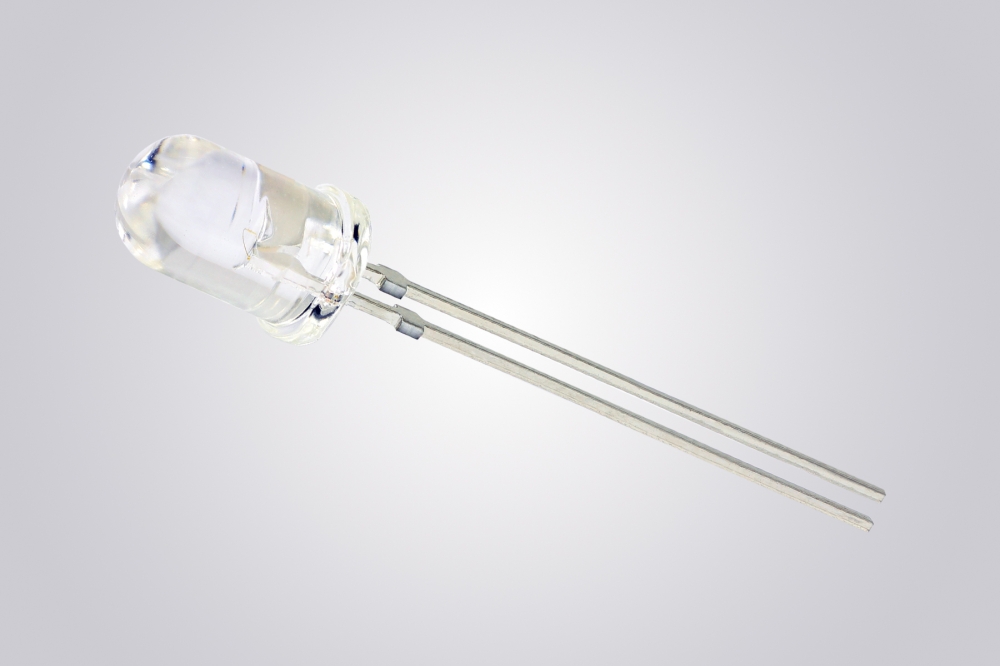
Enhancing efficiency of GaN LEDs with copper substrates
The internal stresses generated when the gallium nitride crystals originally formed on the silicon substrate are reduced when the epilayers are transferred to a copper substrate
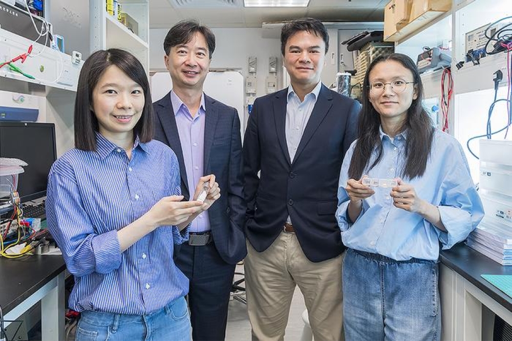
Researchers from Sun Yat-sen University, Guangzhou, China,have succeeded in transferring GaN LEDs grown on a layer of silicon to a layer of copper.
The new copper substrate enabled the GaN crystals to release some of the internal stresses generated when they originally formed. This relaxation helped minimise the so-called "quantum confined Stark effect," a vexing problem for LEDs that reduces their efficiency.
In comparison with LEDs on silicon substrates, the light output of LEDs on copper was enhanced by 122 percent. The relocation of the LEDs produced no obvious deterioration in the crystals' light-emitting region, known as multiple quantum wells.
The researchers attributed the improvements in efficiency to a number of factors. These included the removal of the absorptive substrate, the insertion of a metal reflector between the LEDs' structure and the copper submount. The elimination of electrode shading, which reduces efficiency and the rough surface of the exposed buffer layer, which improves crystal orientation on the substrate, also layed a part .
Further details of this will be described in the paper, "Crack-free InGaN multiple quantum wells light-emitting diodes structures transferred from Si (111) substrate onto electroplating copper submount with embedded electrodes," by Tufu Chen et al, which has been accepted for publication by the American Institute of Physics' journal Applied Physics Letters.