News Article
Tables turn as nature imitates art
Researchers at Northeastern University have grown GaN nanowires which represent a breakthrough in processing them for these novel uses
There are examples of art imitating nature all around us - whether it’s Monet’s pastel Water Lilies or Chihuly’s glassblown Seaforms, the human conception of natural phenomena dazzles but does not often surprise.
Yet when associate professor of physics Latika Menon peered under the electron microscope last fall, she discovered the exact opposite. Instead of art imitating nature, she found nature imitating art.

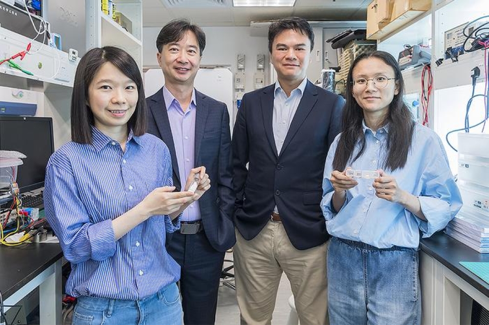
Associate professor Latika Menon and her lab use macroscopic techniques to create nanscopic materials. (Photo by Brooks Canaday)
Menon grew up in the eastern region of India and was vaguely familiar with a cultural dance from the western state of Rajasthan known as the Bhavai pot dance. Nimble dancers sway their hips as a tall stack of wide-bellied pots balances gingerly atop their heads.
Back in the lab at Northeastern, Menon’s team recently created GaN nanowires, which bore a striking resemblance to that stack of pots.
What’s more, a postdoctoral research associate in Menon’s lab, Eugen Panaitescu, jumped on the bandwagon with a cultural art reference of his own. Panaitescu, who hails from Romania, also saw his country’s famous Endless Column reflected in the nanowires.
Dedicated to the fallen Romanian heroes of World War I, Constantin Brancusi’s 96-foot tall monolith is constructed of seventeen three-dimensional rhombuses, periodically wavering from a wider circumference to a narrower one.
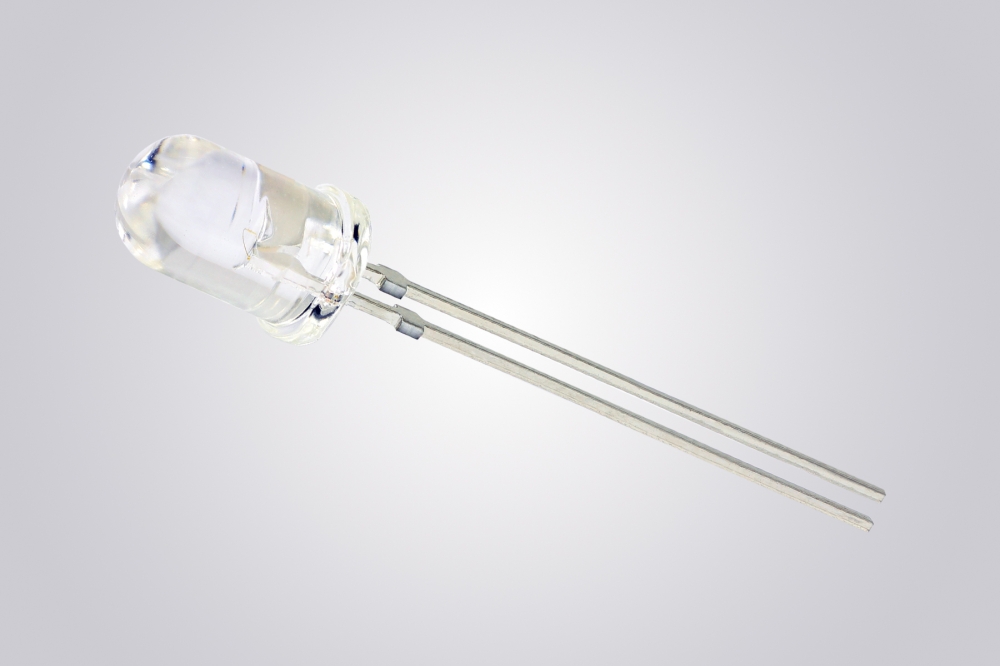
But the Northeastern researchers’ nanowires aren’t just notable for their aesthetic appeal. GaN is used across a range of technologies, including most ubiquitously in LEDs. The material also holds great potential for solar cell arrays, magnetic semiconductors, high-frequency communication devices, and many other things. But these advanced applications are restricted by our limited ability to control the material’s growth on the nanoscale.
The very thing that makes Menon’s nanowires beautiful represents a breakthrough in her ability to process them for these novel uses. She deposited onto a silicon substrate small droplets of liquid gold metal, which act as catalysts to grab gaseous GaN from the atmosphere of the experimental system.
The net forces between the tiny gold droplet, the solid substrate, and the gas cause the nanowire to grow in a particular direction, she points out. Depending on the size of the gold catalyst, she can create wires that exhibit periodic serrations.

Depending on the size of the gold catalyst used to make them, Latika Menon’s nanowires will exhibit periodic grooves that resemble common motifs in art. (Images courtesy of Latika Meno)
“It first tries to grow outward, but that gives the gold a larger surface area,” she says. “So now the wire gets pulled in the inward direction, and then the gold gets a smaller surface area, so it grows outward again.” This inward and outward growth repeated itself again and again to create a periodic structure nearly 6 million times smaller than the endless column and is significantly more promising for its use in advanced devices.
“That there is very little implementation of nanowire technology in electronics or optical devices is due to the fact that it’s very hard to control their shape and dimensions,” says Menon. But now that she has a very simple way of controlling growth, the next step is to control the size of the catalytic droplet with which she starts.
Another advantage of Menon’s approach is using what Panaitescu called “macroscopic techniques” to create nanoscale materials, thus making it scalable and inexpensive. “We just control a few parameters and then leave it, let it do it’s natural thing,” explains Menon.
This work has been detailed in the paper, "Vapor-liquid-solid growth of serrated GaN nanowires: shape selection driven by kinetic frustration," by Zheng Ma et al in Journal of Materials Chemistry C, v. 1 (2013): 2013, 7294-7302. DOI:10.1039/C3TC31776E
Yet when associate professor of physics Latika Menon peered under the electron microscope last fall, she discovered the exact opposite. Instead of art imitating nature, she found nature imitating art.

Associate professor Latika Menon and her lab use macroscopic techniques to create nanscopic materials. (Photo by Brooks Canaday)
Menon grew up in the eastern region of India and was vaguely familiar with a cultural dance from the western state of Rajasthan known as the Bhavai pot dance. Nimble dancers sway their hips as a tall stack of wide-bellied pots balances gingerly atop their heads.
Back in the lab at Northeastern, Menon’s team recently created GaN nanowires, which bore a striking resemblance to that stack of pots.
What’s more, a postdoctoral research associate in Menon’s lab, Eugen Panaitescu, jumped on the bandwagon with a cultural art reference of his own. Panaitescu, who hails from Romania, also saw his country’s famous Endless Column reflected in the nanowires.
Dedicated to the fallen Romanian heroes of World War I, Constantin Brancusi’s 96-foot tall monolith is constructed of seventeen three-dimensional rhombuses, periodically wavering from a wider circumference to a narrower one.
But the Northeastern researchers’ nanowires aren’t just notable for their aesthetic appeal. GaN is used across a range of technologies, including most ubiquitously in LEDs. The material also holds great potential for solar cell arrays, magnetic semiconductors, high-frequency communication devices, and many other things. But these advanced applications are restricted by our limited ability to control the material’s growth on the nanoscale.
The very thing that makes Menon’s nanowires beautiful represents a breakthrough in her ability to process them for these novel uses. She deposited onto a silicon substrate small droplets of liquid gold metal, which act as catalysts to grab gaseous GaN from the atmosphere of the experimental system.
The net forces between the tiny gold droplet, the solid substrate, and the gas cause the nanowire to grow in a particular direction, she points out. Depending on the size of the gold catalyst, she can create wires that exhibit periodic serrations.

Depending on the size of the gold catalyst used to make them, Latika Menon’s nanowires will exhibit periodic grooves that resemble common motifs in art. (Images courtesy of Latika Meno)
“It first tries to grow outward, but that gives the gold a larger surface area,” she says. “So now the wire gets pulled in the inward direction, and then the gold gets a smaller surface area, so it grows outward again.” This inward and outward growth repeated itself again and again to create a periodic structure nearly 6 million times smaller than the endless column and is significantly more promising for its use in advanced devices.
“That there is very little implementation of nanowire technology in electronics or optical devices is due to the fact that it’s very hard to control their shape and dimensions,” says Menon. But now that she has a very simple way of controlling growth, the next step is to control the size of the catalytic droplet with which she starts.
Another advantage of Menon’s approach is using what Panaitescu called “macroscopic techniques” to create nanoscale materials, thus making it scalable and inexpensive. “We just control a few parameters and then leave it, let it do it’s natural thing,” explains Menon.
This work has been detailed in the paper, "Vapor-liquid-solid growth of serrated GaN nanowires: shape selection driven by kinetic frustration," by Zheng Ma et al in Journal of Materials Chemistry C, v. 1 (2013): 2013, 7294-7302. DOI:10.1039/C3TC31776E


