Direct wafer bonding yields large-scale InGaAs-on-insulator transistors
InGaAs grown on a Si donor wafer uses III-V buffer layer
Heterogeneous integration of III-V devices on Si wafers has been explored at length as a way of merging electrical and photonic applications. But existing methodologies have drawbacks such as inferior device quality or high cost in comparison with the current Si-based technology.
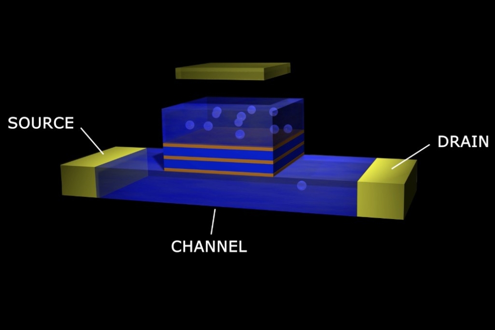
A team of researchers from the University of Tokyo and the companies JST-CREST and IntelliEPI has recently demonstrated InGaAs-on-insulator (OI) fabrication from an InGaAs layer grown on a Si donor wafer with a III-V buffer layer instead of growth on a InP donor wafer.
They report that the InGaAs-OI transistors exhibited high electron mobility of 1700 cm2/V s and uniform distribution of the leakage current, indicating high layer quality with low defect density.
Their paper in Applied Physics Letters explains how the technology allowed them to yield large wafer size scalability of III-V-OI layers up to the Si wafer size of 300mm with a high film quality and low cost. They confirmed the high film quality using Raman and photoluminescence spectra.
![]()
Shown above is the process flow of InGaAs-OI wafers by the DWB technique developed in this study. InGaAs/InxAl1xAs/GaAs layers were epitaxially grown on Si substrates. After Al2O3 deposition as a BOX layer, CMP was carried out for surface smoothing for Al2O3/III-V/Si wafer and wafers were bonded to each other. Subsequent wet etching thinned the top Si and the III-V buffer layers, resulting in the formation of InGaAs-OI on Si substrates.
Heterogeneous integration of III-V compound semiconductors on Si wafers is a key issue for high-performance electrical as well as optical device applications. According to the researchers, In-based III-V compound semiconductors are most preferred channel materials of n-channel transistors for future CMOS circuits due to their high electron injection velocity to replace current Si-based channels facing their physical limitations.
'Direct wafer bonding technology for large-scale InGaAs-on-insulator transistors' by SangHyeon Kim et al appears in Appl. Phys. Lett. 105, 043504 (2014); http://dx.doi.org/10.1063/1.4891493


