NASA to Build First Integrated-Photonics Modem
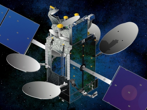
A NASA team is building its first-ever integrated-photonics modem, which it plans to test aboard the International Space Station beginning in 2020 as part of NASA's multi-year Laser Communications Relay Demonstration, or LCRD.
The cell phone-sized device incorporates optics-based functions, such as lasers, switches, and wires, onto a microchip.
Once aboard the space station, the Integrated LCRD LEO (Low-Earth Orbit) User Modem and Amplifier (ILLUMA) will serve as a low-Earth orbit terminal for NASA's LCRD, demonstrating yet another capability for high-speed, laser-based communications.
The LCRD will use lasers to encode and transmit data at rates ten to 100 times faster than today's communications equipment, requiring significantly less mass and power. Such a development could deliver video and high-resolution measurements from spacecraft over planets across the solar system - permitting researchers to make detailed studies of conditions on other worlds, much as scientists today track hurricanes and other climate and environmental changes here on Earth.
The project, which is expected to begin in 2019, isn't NASA's first foray into laser communications. A payload aboard the Lunar Atmosphere and Dust Environment Explorer (LADEE) demonstrated record-breaking download and upload speeds to and from lunar orbit at 622 Mbps and 20 Mbps, respectively, in 2013.
LCRD, however, is designed to be an operational system after an initial two-year demonstration period. It involves a hosted payload and two specially equipped ground stations. The mission will dedicate the first two years to demonstrating a fully operational system, from geosynchronous orbit to ground stations. Once NASA demonstrates that capability, it plans to use ILLUMA to test communications between geosynchronous and low-Earth-orbit spacecraft, Cornwell said.
Recent developments in nanostructures, meta-materials, and silicon technologies have expanded the range of applications for highly integrated optical chips. Furthermore, they could be lithographically printed in mass - just like electronic circuitry today - further driving down the costs of photonic devices.
"This technology will enable all types of NASA missions, not just optical communications on LCRD," Cornwell added.
"We've pushed this for a long time," said Mike Krainak, who is leading the modem's development at NASA's Goddard Space Flight Center in Greenbelt, Maryland. "The technology will simplify optical system design. It will reduce the size and power consumption of optical devices, and improve reliability, all while enabling new functions from a lower-cost system. It is clear that our strategy to leverage integrated photonic circuitry will lead to a revolution in Earth and planetary-space communications as well as in science instruments."
In addition to leading ILLUMA's development, Krainak serves as NASA's representative on the country's first consortium to advance integrated photonics. Funded by the US Department of Defense, the non-profit American Institute for Manufacturing Integrated Photonics, with headquarters in Rochester, New York, brings together the nation's leading technological talent to establish global leadership in integrated photonics. Its primary goal is developing low-cost, high-volume, manufacturing methods to merge electronic integrated circuits with integrated photonic devices.
NASA's Space Technology Mission Directorate (STMD) also appointed Krainak as the integrated photonics lead for its Space Technology Research Grants Program, which supports early-stage innovations.
Demonstrating photonics
Under the NASA project, Krainak and his team will reduce the size of the terminal, now about the size of two toaster ovens. Although the modem is expected to use some optic fibre, ILLUMA is the first step in building and demonstrating an integrated photonics circuit that ultimately will embed these functions onto a chip, he said.
"What we want to do is provide a faster exchange of data to the scientific community. Modems have to be inexpensive. They have to be small. We also have to keep their weight down," Krainak said. The goal is to develop and demonstrate the technology and then make it available to industry and other government agencies, creating an economy of scale that will further drive down costs. "This is the pay off," he said.
Integrated photonics' impact on terrestrial uses is equally profound, Krainak added. One such use is with datacentres. These costly, very large facilities house servers that are connected by fiber optic cable to store, manage and distribute data. "Google, Facebook, they're all starting to look at this technology," Krainak said. "As integrated photonics progresses to be more cost effective than fibre optics, it will be used," Krainak said. "Everything is headed this way."


