Scientists establish mechanism for spin motion in MoS2

Researchers at the National University of Singapore (NUS) and Yale-NUS College have established the mechanisms for spin motion in MoS2, an emerging two-dimensional semiconductor.
They say that their discovery resolves a research question on the properties of electron spin in single layers of 2D materials, and paves the way for the next generation of spintronics and low-power devices. The work was published online in the journal Physical Review Letters on 29 January 2016.
MoS2, a class of transition metal dichalcogenide compounds, has attracted great attention due to wide recognition of its potential for manipulating novel quantum degrees of freedom such as spin and valley.
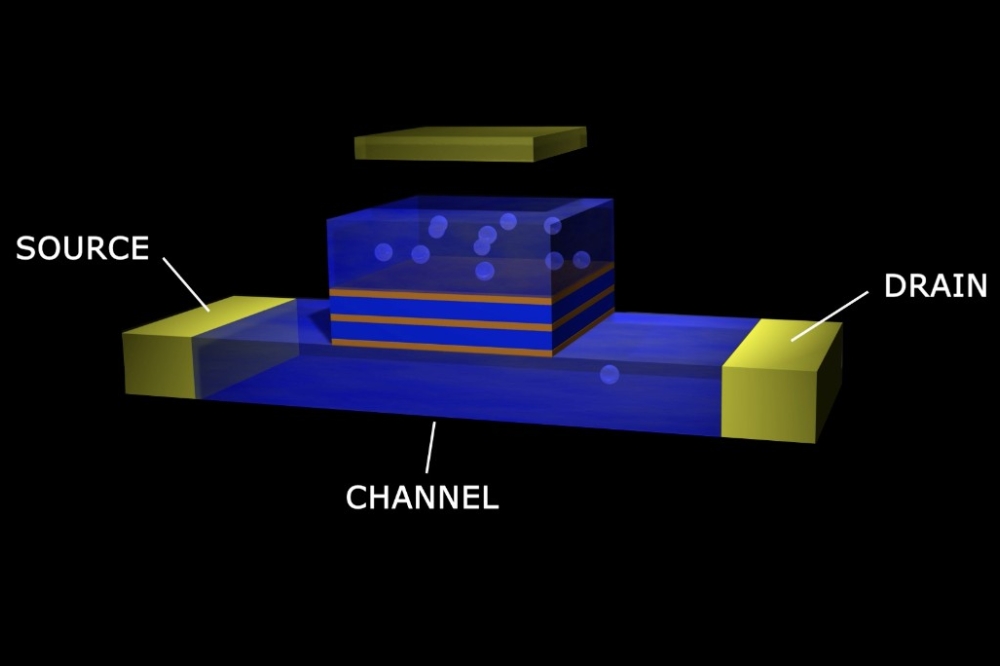
Due to its unique material properties, a single layer of MoS2 has the potential to be used for spin transistors, where both electric current and spin current can be switched on and off independently. Despite this potential for application, there have not been any experimental studies on the mechanism for spin dynamics in MoS2.
To address this gap, scientists from the Centre for Advanced 2D Materials at NUS measured the classical and quantum motion of electrons to extract information on how long spins live in this new material.
The team led by assistant professor Goki Eda, co-leader of this study from the NUS Department of Physics and Department of Chemistry, thinned down a crystal of molybdenite, a mineral of MoS2, to less than one nanometer. The researchers then successfully injected a high density of electrons into this ultra-thin material.
Quantum transport measurements at low temperatures of 2K (-271degC) revealed a surprising transition, where quantum mechanical wave interference switched from constructive to destructive with increasing magnetic field. The team demonstrated that this crossover was caused by spin dynamics.
By comparing the theoretical and experimental results, the two research groups were able to extract spin lifetimes and also determine that the relaxation was driven by the Dyakonov-Perel type where electron spins live longer in dirtier samples.
"Aside from investigating the fundamental properties of low field magnetotransport in MoS2, our team was able to establish the mechanism for spin scattering to reveal the properties of the electron spin," said Hennrik Schmidt, a research fellow working under the supervision of Eda when the study was conducted.
It is hoped that spin-based devices would generally lead to lower energy consumption as compared to conventional electronics.
Yoshihiro Iwasa, director of the Center for Quantum-Phase Electronics at the University of Tokyo, and a world expert on quantum devices who first reported superconductivity in this class of materials remarked: "2D materials have been anticipated as a promising platform for spintronics. I feel that this very comprehensive study of the analysis of the electron spin life time will provide crucial information for further pushing the research toward the realisation of a new generation of spintronic devices."


