Imec Orders Etch and Deposition Systems from Plasma-Therm

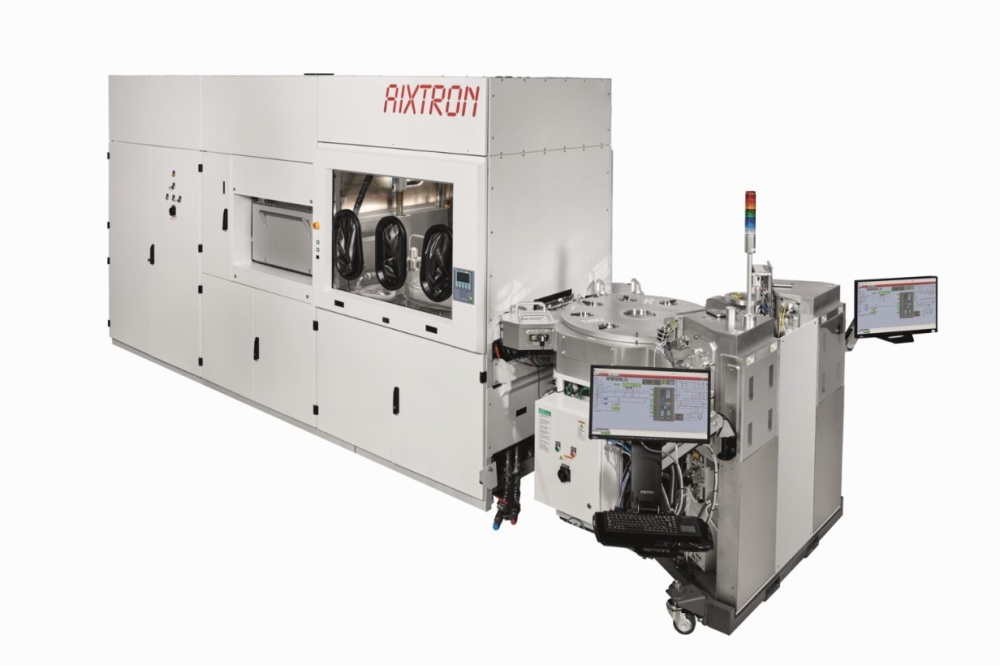
Imec, the Belgium-based, nanoelectronics R&D centre, has ordered two Advanced Vacuum Apex SLR systems from Plasma-Therm, a US-based manufacturer of advanced plasma processing equipment.
One will be configured with an inductively-coupled plasma (ICP) source, with the other configured for high-density plasma chemical vapour deposition (HDPCVD). Apex SLR systems incorporate a field-proven, high-density plasma source that was developed by Plasma-Therm, parent company of Advanced Vacuum, for its widely used Shuttlelock line of plasma tools.
David Lishan, director, technical marketing for Plasma-Therm, noted that: "Plasma-Therm has a long history supporting R&D institutions, and this order continues that tradition. We are pleased that leading R&D organisations rely on Plasma-Therm technology for developing new processes and creating smaller, faster, and more efficient devices."
"It's gratifying that these Apex SLR systems were selected by imec's scientists to help develop industry-relevant technology solutions," Lishan said. Recent Imec innovations include disposable photonics biosensors, flexible electronics, hyperspectral imaging devices, and 3D device integration (advanced packaging) processes.
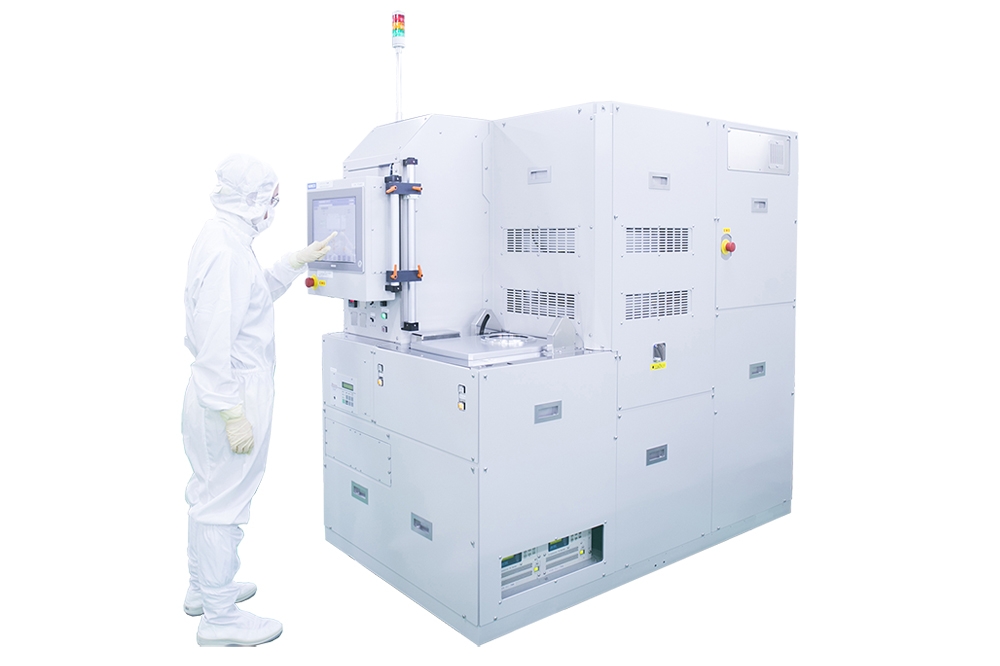
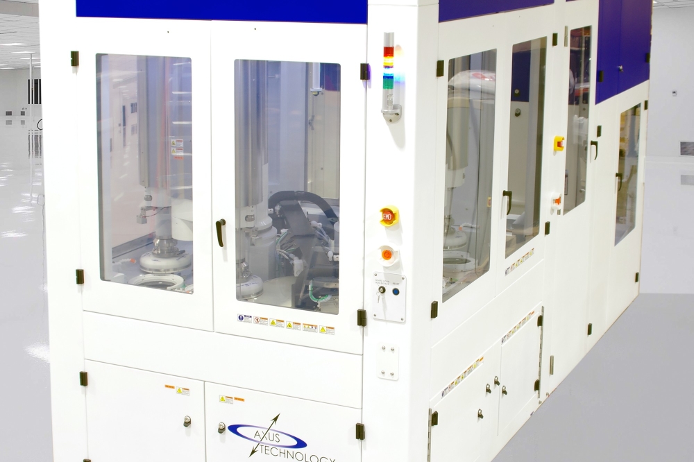
Advanced Vacuum's Apex SLR is described as a highly versatile, small-footprint plasma processing system. Apex SLR ICP is capable of etching a wide range of materials used in semiconductor devices and nanotechnology, while the Apex SLR HDPCVD enables relatively low-temperature plasma deposition of high-quality thin films. These films can include optical coatings, semiconductor device passivation layers, and other materials used in nanoelectronic fabrication and other applications with limited processing thermal budget.


