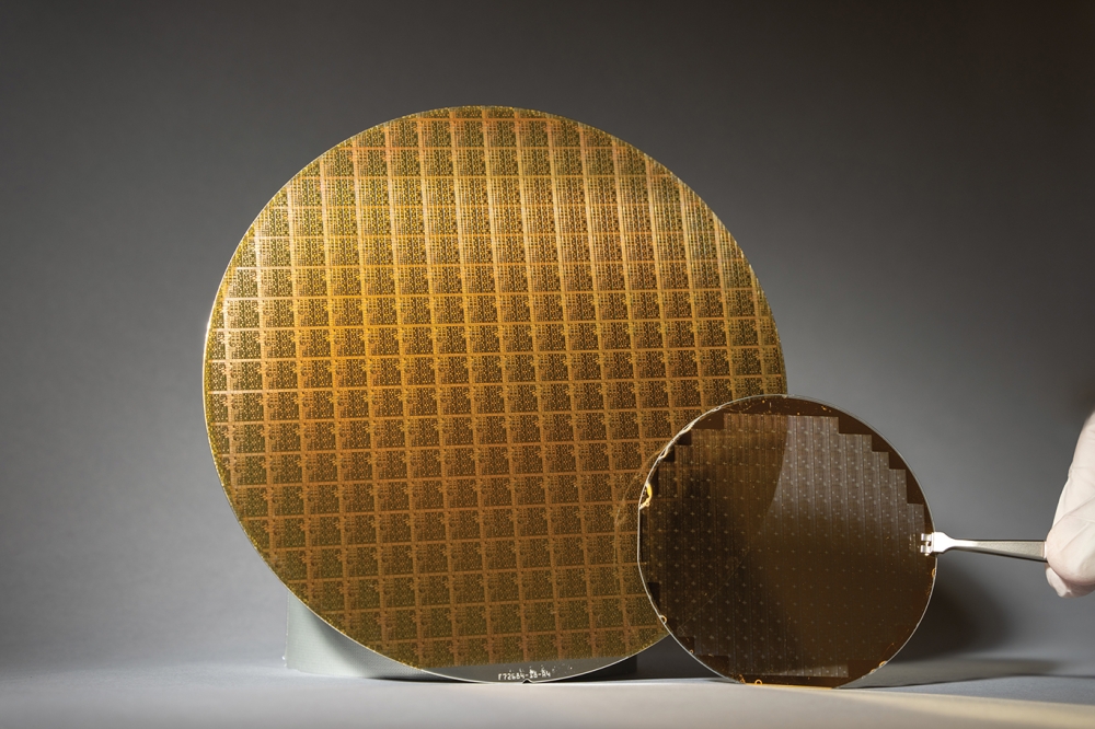
A faster etch for RF devices

As GaN-on-SiC RF devices reach market, Oxford Instruments has delivered a new via etch process to ease fabrication, reports Compound Semiconductor.
For the RF device industry, smooth and fast SiC backside via etching is crucial to high performance, cost-effective semiconductors.
Just last month, Oxford Instruments revealed its latest SiC via etch process to be added to the PlasmaPro100 Polaris etch system.
Already designed to deliver fast etch rates on GaN, Sapphire, SiC wafers and more, the single wafer etch system now promises a faster, smooth via etch through SiC at a time when the wide bandgap material is proving crucial to the development of GaN-on-SiC RF devices.
"The system was released a couple of years ago now but this SiC via process is new," says Mark Dineen, Optoelectronics Product Manager at Oxford Instruments Plasma Technology.
"We saw a market need for this, developed it and believe now is the time to release it," he adds. "GaN-on-SiC is definitely a growing market and we want to be part of that."
But the road to the smooth SiC via hasn't been straightforward. SiC backside via etching is crucial to form a contact with electrodes during the fabrication of GaN-on-SiC transistors. However SiC is a tough material to etch and researchers worldwide have grappled with how best to handle a substrate with a hardness close to that of diamond. Oxford Instruments now believes it has the answer.
New steps
As part of the latest etch process, the SiC is mounted onto a sapphire carrier using wax, ready to plasma-etch the via some 100 microns through the wafer. As Dineen highlights, this wafer thickness demands a fast, aggressive etch, and as such, process engineers at Oxford Instruments have opted for a 1.2 micron per minute etch rate.
"We need smooth sidewalls in the via, and if we went faster, we would produce jagged features within the via which leads to localised heating and reduces device lifetime," he says. "But any slower, then throughput is just too slow and the [system] cost of ownership is too high."
A key issue that many researchers have encountered while optimising SiC substrate via etch processes is the formation of so-called pillars in the via hole, which impede metallisation. These unusual structures form on the end of micro-pipes - hollow tubes that are created during SiC growth - and are exposed after the relatively thick SiC wafer is chemically thinned to around 100 micron for the via etch.
Myriad researchers have experimented with pre-etch clean and etch processes to avoid pillar formation. But according to Dineen, Oxford Instruments has countered this problem by introducing a 30 second etch to the process that smoothly removes the top layer and accompanying defects to produce a clean surface prior to the main SiC via etch.
![]()
Oxford Instrument's latest via etch process promises a via with smooth, slightly sloping sidewalls for high performance devices.
So, with defects removed, the relatively fast, aggressive plasma-etch swiftly produces a smooth, slightly sloped via, ready for post-etch metallisation. However, this process also generates heat around the wafer and sapphire carrier, spelling bad news for the all-important wax attachments that have an upper temperature limit of 150°C.
To maintain wax integrity, the wafer is electrostatically clamped to a lower electrode, which contains liquid cooling channels to transfer heat away through the electrode. As Dineen highlights, electrostatic clamping is widely used in the silicon industry, but during this SiC via etch process, a non-conducting sapphire substrate is being handled that will adhere to the clamp at the end of the etch.
Given this, the company transferred a technology to the system that was developed as part of its past GaN-on-sapphire LED research.
"We had developed an electrostatic clamp that could efficiently clamp bare sapphire as part of our patterned sapphire substrate process," explains Dineen. "Thanks to the control method we developed here we have excellent cooling in our system and the wafers are handled very smoothly."
While the company capitalises on lessons learned from LED process development, does it also expect the up and coming GaN-on-SiC RF device market to provide the same potential for growth? Dineen points to the likes of Wolfspeed, Panasonic and Fujitsu, all developing GaN-on-SiC RF devices, and also highlights how China-based manufacturers are now penetrating the market.
Yet, an LED-type boom isn't expected. As Dineen puts it: "We do see a lot of growth in this market but I don't think we will see anything quite as big as the LED market."
"This is an interesting market, it's growing and SiC also has potential in power applications," he adds. "This all ties in with our expertise around III-V materials in these niche production markets."
And what about rival GaN-on-silicon devices? For example, this time last year, MACOM celebrated shipping more than one million GaN-on-silicon RF devices while claiming a 100W transistor with comparable performance at a cheaper cost. And more recently, imec has launched a GaN-on-silicon research program to produce eight inch wafers.
"Processing costs will be a barrier for GaN-on-SiC devices but its performance is driving demand," he says. "If you measure GaN-on-SiC device quality versus cost, it is a strong choice compared to GaN-on-silicon. GaN-on-silicon will have a place for sure, although there are limitations on performance."
Still, Oxford Instrument's PlasmaPro100 Polaris etch system can handle wafer sizes up to eight inches. And as Dineen concludes: "I'm not sure whether or not SiC wafers will reach that diameter, but GaN-on-silicon wafers are getting there, so we can etch a GaN recess into these wafers if needed."


