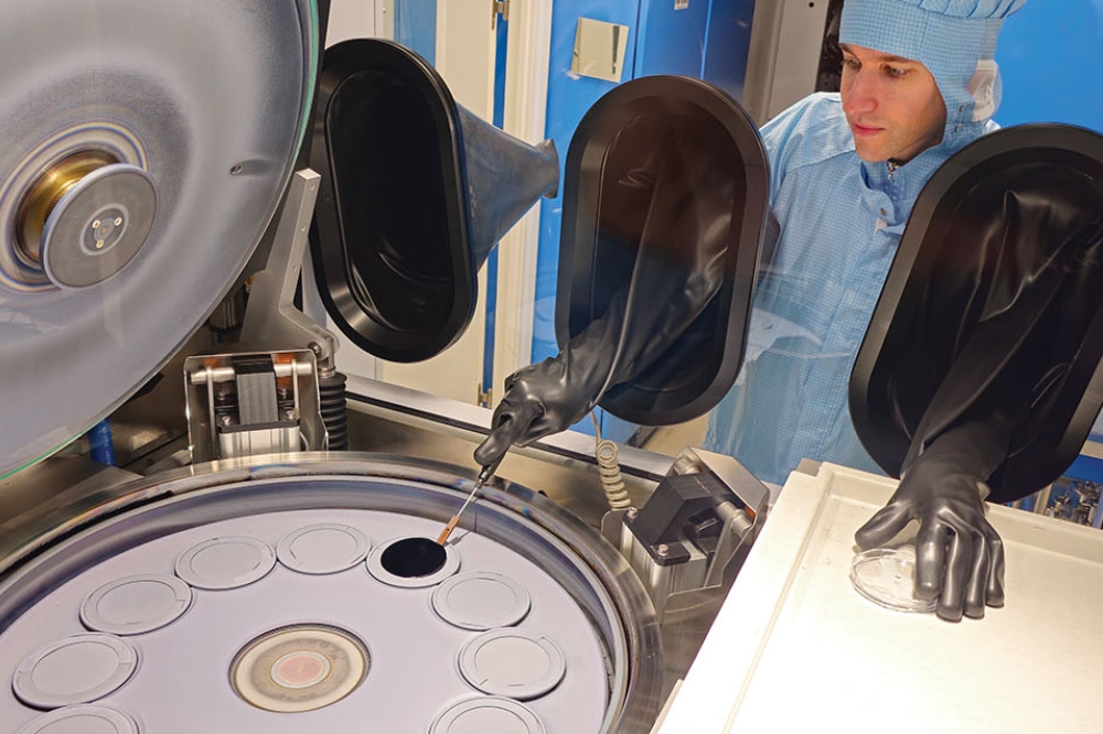
$3M Penn State grant for power GaN research

Rsearchers at Penn State University will receive $3 million from the US Defense Advanced Research Projects Agency (DARPA) as part of a larger grant awarded to Northrop Grumman, a defence, aerospace and technology company.
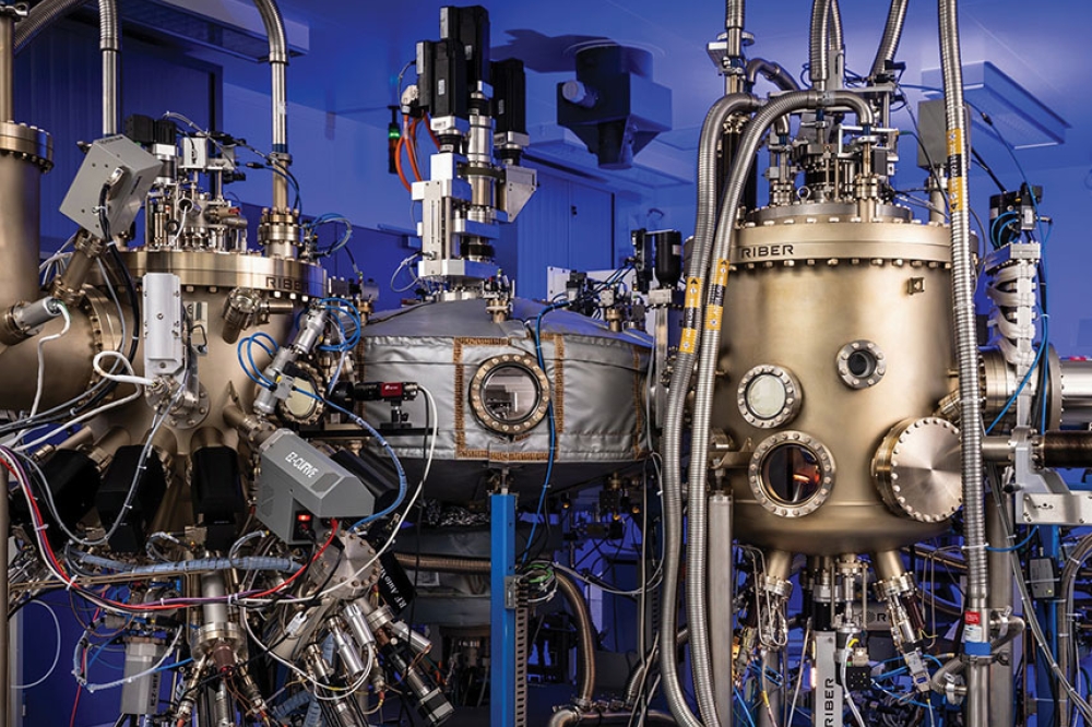
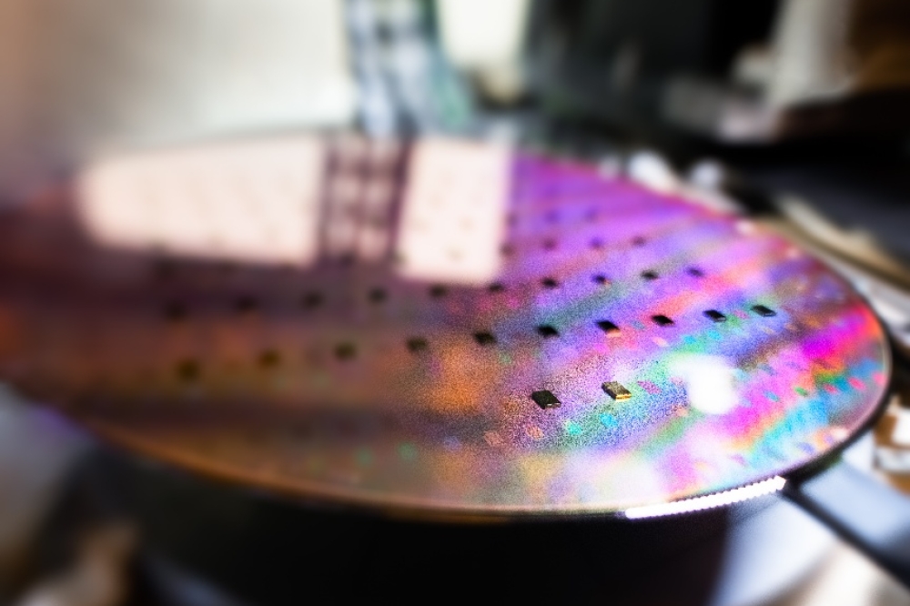
The joint project will aim to develop a novel method for integrating GaN with silicon substrates using 2D materials as interlayers.
According to the researchers, this hybrid approach can lead to more efficient power electronics with lower production costs, making them ideal for high-demand applications like electric vehicles, power electronics and data centres, where efficiency and durability are critical.
“Silicon is the common platform for microelectronics but it is challenging to combine new semiconductor materials with silicon,” said Joan Redwing, distinguished professor of materials science and engineering and director of the Penn State Materials Research Institute’s (MRI) Two-Dimensional Crystal Consortium, a US National Science Foundation Materials Innovation Platform and national user facility.
She added: “To overcome this, we need new approaches to densely integrating advanced materials with silicon, and that is exactly what this project is about. Our work with Northrup Grumman is designed to explore integrating GaN directly onto silicon using 2D materials as interlayers.”
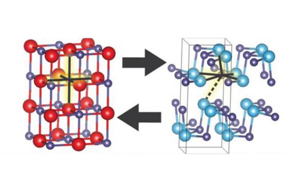
With the DARPA grant, Penn State researchers will work with Northrup Grumman to use 2D materials such as MoS2 and GaSe as 'seed layers' to grow GaN on industry compatible silicon (001). Silicon (001) is the preferred crystal orientation used in current semiconductor technology. A seed layer provides a template or foundation that influences the structure, orientation and quality of the material grown on top.
“The current approach to GaN-on-silicon integration has too many drawbacks, from increased thermal resistance to device fabrication challenges on silicon (001),” said Joshua Robinson, professor of materials science and engineering and Penn State’s principal investigator on the DARPA project. “By using 2D materials as seed layers, we aim to eliminate these issues and develop a direct route to integrating gallium-nitride-on-silicon with improved performance compared to current technologies. This could directly impact manufacturing costs and enable market entry into energy-efficient devices.”
“This program allows us to demonstrate that 2D materials could be key to enabling advances in 3D semiconductors,” Robinson said. “We’re combining our expertise in 2D research with the real-world need for improved semiconductor performance, setting the stage for years of innovation in heterogeneous integration.”