Riber celebrates 60 years of success

With a pedigree in vacuum technology stretching back 60 years, Riber has an enviable track record in MBE innovation that shows no signs of abating.
BY CLAUDINE PAYEN FROM RIBER
Engineering companies operating at the cutting edge of technology are renowned for their precision. Such firms are built on calculation, with every alteration accounted for. There’s little room, if any, for uncertainty.
So it’s almost unthinkable that given all this attention to detail, one such outfit is shrouded in a mystery since its conception. But that’s the case for Riber, our company that’s a pioneer of MBE, and now celebrating its 60th anniversary.
What, you may ask, is the nature of this mystery? Well, it is the reason behind the name of the company, founded by four engineers in 1964. There is no apparent connection between any of them and the name of our company.
Looking back on those formative years, what is known is the initial focus, a combination of stainless-steel fabrication and tungsten-inert-gas welding for high-vacuum applications, an emerging technology of the time. Alongside this, we distributed American-made micro-welders and ion pumps.
Riber’s first MBE system. Photo from 1980.
Like many small and successful start-ups, we quickly expanded our portfolio. Three years in, we started to make Joule-effect evaporators, vacuum chambers and a series of accessories. It’s a direction of travel that continued into the 1970s, when our design office would draw plans for increasingly complex chambers. Such work drove our first technological shift, as we moved into the production of analytical instruments, such as Auger spectroscopes and low-energy electron diffraction systems.
During this time of transition, our clientele expanded from research laboratories to include industrial companies. We also developed new accessories, such as valves, ultra-high vacuum (UHV) linear and rotary feedthroughs, and many other components.
Pioneering MBE
A major milestone came in 1974, when we created a unique system at the request of the now legendary pioneer of MBE, Klaus Ploog, who had just started leading a group at the Max Planck Institute for Solid-State Research in Stuttgart, Germany. Using the UHV chamber we provided, Ploog and his co-workers were able to deposit arsenic and gallium via evaporation. Their efforts led to the development of the first Knudsen cells, comprising a graphite crucible 2 cm³ to 3 cm³ in size, accompanied by a thermocouple and a heating element spiralled around machined alumina. Samples produced in this chamber were just 10 mm in size.
Our driving force behind these fledgling MBE tools is Pierre Bouchaïb, the product manager during our formative years. While the nature of the growth in this chamber was yet to be christened MBE, this work marked the beginning of increasing interest in this technology from laboratories like IBM, Bell Labs, NEC, Rohm and Sony. All would go on to play a key role in the development of this class of epitaxy.
From these early days onwards, MBE has advanced in both its capability and the performance of the growth tools. Critical to this progress are the partnerships that we have formed with our users. We have a deep commitment to collaboration, which is part of our core values. As Bouchaïb used to say: “Our only limit is the imagination of our clients.”
The starting assembly room. Photo from 1964
As interest in MBE expanded throughout the 1970s and beyond, with research groups keen to explore the mechanisms behind the growth of material, we shipped more and more systems. Often designed for research, they could accommodate substrates up to 2 inches in diameter, but would often be used to produce epilayers on smaller platforms.
During the 1980s, we reached a manufacturing milestone, passing the production of 100 systems sold in 1984, and we also received a strong endorsement from a master of MBE, Al Cho. Often referred to as the father of this particularly growth technology for his trailblazing work at Bell Labs, Cho visited our headquarters on the outskirts of Paris during the 1980s, and paid tribute to the key features of our MBE tool. He argued that the best MBE machines should exclusively feature a liquid-nitrogen cooling unit, cells and a manipulator, as anything else was a source of contamination. Our systems are built around these core principles.
From research to industrialisation
Inspired by scientific discoveries, many new commercial applications related to compound semiconductor devices have emerged since the 1990s. To support this, we have expanded our portfolio, introducing more industrial machines. This includes the MBE 49, our first fully automated industrial prototype, unveiled in 1990. Developed for the company Bandgap in the US, this reactor broke new ground by enabling several substrates to be grown simultaneously.
We have also advanced our effusion cell technologies. A great deal of progress has been made with valve cells for cracking group V elements, enabling a significant increase in the arsenic incorporation on substrates; and we have also improved cells for group III elements, which now offer capacities of several hundred cubic centimetres.
A key juncture in our history came in 1994, when we decided to focus exclusively on producing MBE systems. At this point in time we divested our instrumentation division, now known as the company Cameca. Back in the early 1990s, our portfolio included secondary ion mass spectrometers, instruments for Auger spectroscopy, and low-energy electron diffraction systems.
Our focus on MBE has helped us in our efforts to develop new tools. In 1997 we launched the MBE 6000, which offers double the capacity of the MBE 49. This hit the market at a time when production systems in an industrial setting were gaining substantial traction, with around 50 already operating worldwide.
Throughout our history, we have continued to innovate, never resting on our laurels. This willingness to keep pursuing excellence and questioning what might be best has led us to some fundamental changes. Through a project called ANISET, named after a spirit that’s well known and appreciated in the south of France and has the taste of aniseed, we worked with Jean Massies and his team at CRHEA in the late 1990s to transition MBE reactors from a horizontal to a vertical design. Since then, this new geometry has become the standard for MBE growth.
Today we offer an extensive range of MBE reactors for research and production. Our focus is on improving the reproducibility, stability and uniformity of our machines, goals that we are helping to fulfil through sustained work on manipulators and cells. Through our acquisition of Addon in 2008, we have expanded our product range to include RF cells, as well as cells designed specifically for corrosive materials, such as antimony, magnesium and tellerium. Another advance is our introduction of a ‘cluster’ version of our machines, providing full flexibility and automation. This move has been motivated by the emergence of centres of excellence, and the pooling of machines by multiple working groups.
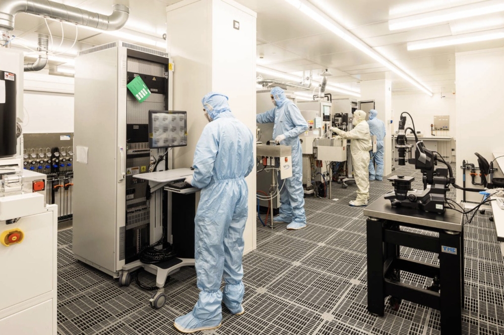
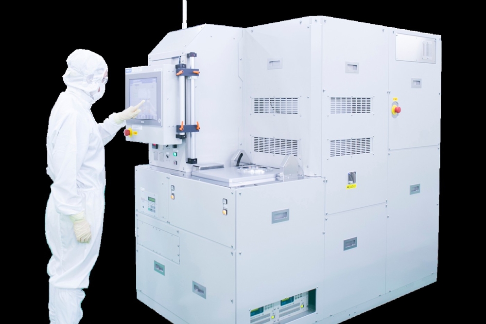
Today’s cleanroom at Riber, featuring an MBE 6000 system.
Silicon photonics and quantum materials
Last year, we launched the highest capacity machine on the market: the MBE 8000. This highlights how we have come full circle, from the most advanced research machine to the most demanding production system.
Today, as well as selling state-of-the-art MBE tools, we also offer the hardware to support exceptional epitaxy. We provide our clients with real-time, in-situ control, featuring feedback loops on all growth parameters, thanks to a range of optical instruments called EZ-Tools that are compatible with our entire product range.
The capability of our instrumentation never stands still, thanks to ambitious development at Epicentre, a joint laboratory between ourselves and LAAS-CNRS.
We are also playing a key role in emerging technologies, such as silicon photonics. We are developing a platform called ROSIE - Riber oxide silicon epitaxy – that will enable the growth of barium titanate on 300 mm silicon substrates. It’s a project that’s addressing the challenge of the adoption of this technology in high-volume silicon fabs.
Alongside this, we are finalising the validation of a quantum platform that combines standard epitaxy with 120 K epitaxy to produce superconducting materials. Over the coming months we shall start to offer this opportunity to the MBE community.
Like the compound semiconductor industry, we have come through some challenging periods. But drawing on 60 years of success, we continue to be a key player, ready to tackle the challenges that will lie ahead for the next 60 years.

