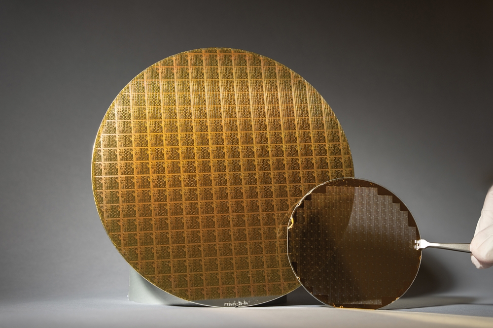
Carbonics introduces carbon-on-silicon solution for RF components
Venture-backed startup Carbonics, has launched its ZEBRA carbon-on-silicon technology for radio frequency (RF) components and devices in the rapidly expanding wireless, communications, defence and aerospace markets.
Carbonics is focused on developing and commercialising a carbon-on-wafer single chip solution that could, the company says, vastly improve the power consumption and performance of wireless products including next-generation smartphone and communication devices.
The ZEBRA product is the first available platform solution for realising next-generation semiconductor devices technologies using the novel material of semiconducting single-walled carbon nanotubes (CNT). By leveraging the superior one-dimensional (1D) transport properties of thousands of aligned, gate-controllable conduction pathways, linear current densities exceeding that of GaAs pHEMT (gallium arsenide metamorphic high electron mobility transistor) and silicon technologies have been realised.
Ultra-arrayed carbon nanotubes represent the enabling technology necessary for a carbon-on-wafer single chip solution, and the launch of the ZEBRA wafers remains in step with Carbonics' mission to enable design engineers, foundries, integrated device manufacturers and advanced development houses access to the best and most advanced semiconducting platform for designing next-generation high speed circuits.
"Carbonics intends to shake up the billion-dollar compound semiconductor market with our superior disruptive carbon technology that is fully CMOS compatible and able to perform in the mmWave spectrum"”representing perfect timing for the 5G and Internet of Things (IoT) revolution," said Carbonics CEO Kos Galatsis.
"Carbonics has achieved a unique milestone in the evolution of carbon electronics," said Ken Hansen, President and CEO of Semiconductor Research Corporation (SRC). "This is a crucial first step from Carbonics toward high performance, next-generation RF electronics using next-generation nanotechnology for high performance mmWave RF and CMOS compatibility. It's exciting to see the progress from the fundamental material and device research sponsored by SRC and DARPA develop into the launch of a groundbreaking product technology."
The ZEBRA wafer product line includes the ZEBRA BOLT with aligned semiconducting CNT on 15 nm SiO2 for backgated device applications such as sensors and detectors; the ZEBRA DASH with aligned semiconducting CNT on 1500nm for top-gated devices such as memory, switch, logic and RF applications covering L-Band to mmWave and 3G, 4G, 4G, WiFi, 802.11ad and WiGig spectrums; and the "ZEBRA SPRINT" with aligned semiconducting CNT on quartz aimed for RF applications up to 100 GHz. The ZEBRA products can be purchased online at www.carbonicsinc.com.
Carbonics also plans to launch its VIPER product line made up of high performance RF devices and integrated amplifiers in 2017 and its STINGRAY product line of RFICs and MMICs that will include high performance mmWave LNA, PAs, mixers, switches and front-end modules (FEMs) in 2018.
Started in 2014, the Los Angeles-based Carbonics is backed by a $5.5 million investment from TAQNIA International. Carbonics was spun-out from UCLA and USC and funded by university-sponsored research from the Centre of Excellence for Green Nanotechnologies at UCLA and King Abdulaziz City for Science and Technology Centre (KACST), SRC, DARPA, U.S. Air Force and UCLA's California NanoSystems Institute Technology Incubator.


