'Lossless' metamaterial could boost laser efficiency
University of Californoia team add InGaAsP to produce material that behaves as a metal and a semiconductor
![]()
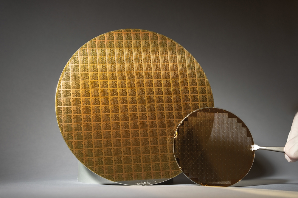
SEM images of 'lossless' metamaterial
Engineers at the University of California San Diego have developed a material that could reduce signal losses in photonic devices. They think the advance has the potential to boost the efficiency of lasers, photovoltaics, and fibre optic communication systems.
The discovery addresses the problem of how to minimise loss of optical signals in plasmonic metamaterials.
Plasmonic metamaterials are engineered at the nanoscale to control light in unusual ways. But they typically contain metals that absorb energy from light and convert it into heat. As a result, part of the optical signal gets wasted, lowering the efficiency.
In the recent study "˜Luminescent hyperbolic metasurfaces' published in Nature Communications, the researchers led by Shaya Fainman demonstrated a way to make up for these losses by incorporating the light emitting compound semiconductor InGaAsP into the metamaterial.
"We're offsetting the loss introduced by the metal with gain from the semiconductor. This combination theoretically could result in zero net absorption of the signal - a 'lossless' metamaterial," said Joseph Smalley, an electrical engineering postdoctoral scholar in Fainman's group and the first author of the study.
In their experiments, the researchers shined light from an infrared laser onto the metamaterial. They found that depending on which way the light is polarised, the metamaterial either reflects or emits light.
"This is the first material that behaves simultaneously as a metal and a semiconductor. If light is polarised one way, the metamaterial reflects light like a metal, and when light is polarised the other way, the metamaterial absorbs and emits light of a different 'colour' like a semiconductor," Smalley said.
Researchers created the new metamaterial by first growing a crystal of InGaAsP on a substrate. They then used high-energy ions from plasma to etch narrow trenches into the semiconductor, creating 40nm-wide rows of semiconductor spaced 40nm apart. Finally, they filled the trenches with silver to create a pattern of alternating nano-sized stripes of semiconductor and silver.
"This is a unique way to fabricate this kind of metamaterial," Smalley said. Nanostructures with different layers are often made by depositing each layer separately one on top of another, "like a stack of papers on a desk," Smalley explained. But the semiconductor material used in this study can't just be grown on top of any substrate (like silver), otherwise it will have defects. "Rather than creating a stack of alternating layers, we figured out a way to arrange the materials side by side, like folders in a filing cabinet, keeping the semiconductor material defect-free."
As a next step, the team plans to investigate how much this metamaterial and other versions of it could improve photonic applications that currently suffer from signal losses.


