GaNonCMOS project to drive power integration densities

German PCB firm AT&S has announced that it is one of a number of organisations collaborating within a new Horizon 2020 EU Research and Innovation programme called GaNonCMOS, coordinated by Jean-Pierre Locquet from the Katholieke Universiteit Leuven (KUL).
EpiGan, Fraunhofer, IBM Research, IHP, Tyndall National Institute, PNO Innovation, Recom, NXP Semiconductors and X-FAB Semiconductor are the other participants.
The four year project, launched in January 2017, aims to bring GaN power electronic materials, devices and systems to the next level of maturity by providing the most densely integrated materials to date.
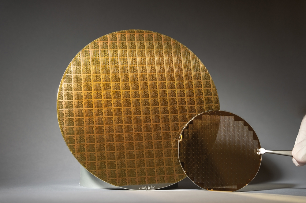
This will be realised by integrating GaN power switches with CMOS drivers using different integration schemes from the package level up to the chip level including wafer bonding between GaN on Si(111) and CMOS on Si (100) wafers.
The project aims to produce several demonstrators with GaN power switches and CMOS drivers, as well as new magnetic core materials that will enable switching frequencies up to 200 MHz.
Combined with optimised embedded PCB technology, the developments should lead to new integrated power components for low-cost, high-reliability systems, according to AT&S.


