
Gallium oxide: ready to take on GaN and SiC
Following massive investor funds, Flosfia is poised to deliver high performance, affordable gallium oxide devices, reports Rebecca Pool.
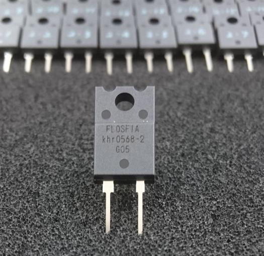
Flosfia devices will first be used in power factor correction applications [Flosfia]
In early March, this year, Kyoto University start-up, Flosfia, revealed it had won an incredible JPY 750 million - £5.4 million - in finance to commercialise corundum structured gallium oxide Schottky barrier diodes and MOSFETs.
With the ample funds coming from investors, old and new - including Yaskawa Electric, Future Venture Capital, Energy & Environment Investment and more - Flosfia will now develop its own production lines with a view to launching commercial production in 2018.
"We have existing, new and strategic investors in this round of funding which is a great sign for our technology and reflects that we are moving forward," highlights Takuto Igawa, vice president of marketing at Flosfia. "Yaskawa is one of the biggest industrial global businesses in the world and they have joined us as an investor and also a user of our devices."
Flosfia was founded in March 2011, by Kyoto University researchers, Toshimi Hitora, Shizuo Fujita and Kentaro Kaneko to commercialise a CVD process called 'Mist Epitaxy'. As the rest of the world grappled with the epitaxial growth of GaN or SiC, the researchers had developed a novel method to deposit layers of gallium oxide onto sapphire substrates, to fabricate power devices.
Ga2O3 comes in five different phase phases with its α-phase taking the same corundum crystal structure as Al2O3 or sapphire, opening the door to stress-free epitaxy of Ga2O3 layers on sapphire substrates.
Indeed, as early as 2008, Flosfia co-founder and technology pioneer, Professor Shizuo Fujita, was successfully depositing thin films of α-Ga2O3 onto sapphire substrates. And today, the refined growth process produces dislocation-free epilayers on four inch sapphire substrates, a critical step towards reaching cost-parity with the industry incumbent, silicon.
 Flosfia chief executive, Toshimi Hitora, is ready to take gallium oxide schotty barrier diodes and MOSFETs to market. [Flosfia]
Fujita and colleagues at Flosfia have also developed a 'lift-off' proprietary process to transfer the α-Ga2O3 layers from the sapphire substrate to a high thermal conductivity metal support, alleviating the thermal management issues that plague SiC and GaN power devices.
The researchers claim the process has been honed for the high throughput and easy-handling of wafers. And as Flosfia external director, Naonori Kurokawa highlights: "Using the sapphire substrate is much much cheaper than using a silicon carbide substrate.
"We cannot disclose details of our lift-off process, but we can say it does not cause a bottleneck in fabrication, so we will be ready for commercial supply," he adds.
From a device point of view, Ga2O3 also has a Baliga figure of merit some twenty times higher than SiC. And crucially for myriad applications, the ceramic oxide has a bandgap energy of around 5 eV, much higher than that of SiC and GaN, which both come in at just less than 3.5 eV.
As a result, such a ceramic oxide device can achieve a higher operating voltage and lower on-resistance than the SiC or GaN equivalent, as Flosfia demonstrated with its first Schottky barrier diode (SBD) in 2015. The 521 V device had an on-resistance of 0.1 mΩcm2, lower than that of any commercially-available SiC diode.
Remarkably, the company released a 855V Schottky barrier diode, around the same time, with an on-resistance of 0.4 mΩcm2.
"We're are only a six-year-old start-up but we have already beaten the on-resistance world record," says Kurokawa. "What's more our 600V, 5A device is almost ready. Development in the last couple of years has been huge."
Towards commercialisation
Right now, Flosfia is sampling SBDs in industry standard TO-220 packages with its industrial partner, Japan-based robotics manufacturer, Yaskawa Electric, with a view to delivering commercial devices in 2018.
"Based on our sample tests we will soon determine the final product specification," says Igawa. "Our 600V, 5A device will be coming very soon now."
The company also aims to sample MOSFETs in 2019, taking these to commercial production from 2020. "We will target markets all over the world, and our first product, the 600V, 5A diode, will be used for power factor correction," says Igawa.
As device development and performance continues apace, Flosfia still has to deliver on one key factor; cost. From the outset, the company stated it would deliver devices at a cost to match the silicon equivalent, and according to Flosfia president, Toshimi Hitora, this is coming.
"We are still in our research and development phase so we can't confirm costs yet but come mass production of our Schottky barrier diodes in 2018, I know we will reach cost-parity with GaN and SiC devices," he says. "We then intend to reach cost-parity with silicon in 2019."
"MIST-EPITAXY is a safe, low-cost and energy-saving technology for growing oxide semiconductors to suppress device cost so power devices can become ubiquitous," he adds.


