US team uses GaN and InGaN nano-sandwich to upconvert light

Efficient upconversion of light could let solar cells turn otherwise-wasted infrared sunlight into electricity
A US team has combined plasmonic metals and semiconducting quantum wells to efficiently boost the frequency of light. Upconversion of light in this way could let solar cells turn otherwise-wasted infrared sunlight into electricity or help light-activated nanoparticles treat diseased cells, according to the researchers.
The development uses nanoscale pylons made of alternate layers of GaN and InGaN topped with a thin layer of gold and surrounded by silver. When these are struck by green light they produced a higher-energy blue glow.
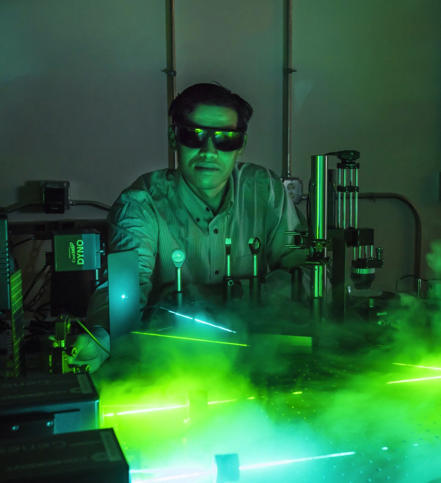
"I'm taking low-energy photons and converting them to high-energy photons," said Gururaj Naik, an assistant professor of electrical and computer engineering at Rice University who developed the prototype while at the Stanford lab of Jennifer Dionne. The work appears in the American Chemical Society's Nano Letters.
The pylons measure about 100nm across. When excited by a specific wavelength of light, specks of gold on the tips of the pylons convert the light energy into plasmons, waves of energy that slosh rhythmically across the gold surface like ripples on a pond. Plasmons are short-lived, and when they decay, they give up their energy in one of two ways; they either emit a photon of light or produce heat by transferring their energy to a single electron - a 'hot' electron.
Naik's work at Stanford was inspired by the work of Naomi Halas and Peter Nordlander at Rice's Laboratory for Nanophotonics, who had shown that exciting plasmonic materials also excited electrons and holes within.
"Plasmonics is really great at squeezing light on the nanoscale," said Naik, who joined Rice's faculty a year ago. "But that always comes at the cost of something. Halas and Nordlander showed you can extract the optical losses in the form of electricity. My idea was to put them back to optical form."
In Naik's design the hot electrons and hot holes are directed toward the GaN and InGaN bases that serve as electron-trapping quantum wells. These wells have an inherent bandgap that sequesters electrons and holes until they recombine at sufficient energy to leap the gap and release photons at a higher frequency.
Present-day upconverters used in on-chip communications, photodynamic therapy, security and data storage have efficiencies in the range of 5 to 10 percent, Naik said. Quantum theory offers a maximum 50 percent efficiency ("because we're absorbing two photons to emit one") but, he said, 25 percent is a practical goal for his method.
Naik noted his devices can be tuned by changing the size and shape of the particles and thickness of the layers. "Upconverters based on lanthanides and organic molecules emit and absorb light at set frequencies because they're fixed by atomic or molecular energy levels," he said. "We can design quantum wells and tune their bandgaps to emit photons in the frequency range we want and similarly design metal nanostructures to absorb at different frequencies. That means we can design absorption and emission almost independently, which was not possible before."
"That's a solid-state device," Naik said of the prototype. "The next step is to make standalone particles by coating quantum dots with metal at just the right size and shape."
These show promise as medical contrast agents or drug-delivery vehicles, he said. "Infrared light penetrates deeper into tissues, and blue light can cause the reactions necessary for the delivery of medicine," Naik said. "People use upconverters with drugs, deliver them to the desired part of the body, and shine infrared light from the outside to deliver and activate the drug."
The particles would also make a mean invisible ink, he said. "You can write with an upconverter and nobody would know until you shine high-intensity infrared on it and it upconverts to visible light."
'Hot-Carrier-Mediated Photon Upconversion in Metal-Decorated Quantum Wells', by Naik et al; Nano Lett., June 29, 2017


