
2D materials can multitask
New process produces patterned monolayers for creating materials with dual optical, magnetic, catalytic or sensing capabilities
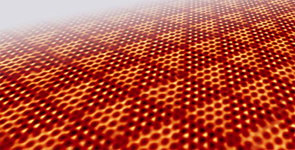
Sokrates Pantelides, a professor of Physics at Vanderbilt University, and Hong-Jun Gao at the Institute of Physics of the Chinese Academy of Sciences in Beijing have shown that monolayers formed by two chalcogenides (PtSe2 and CuSe) naturally combine with nanoscale precision into alternating triangles with different phases: metallic and semiconductor.
Because each phase has different electrical and chemical properties, two different types of molecules can bond to its surface, allowing it to perform two functions simultaneously.The researchers grew the monolayer of PtSe2 on a Pt substrate and the monolayer of CuSe on a Cu substrate.
Their paper 'Intrinsically patterned two-dimensional materials for selective adsorption of molecules and nanoclusters' was published Jun. 12 in the journal Nature Materials.
"In general, 2D materials are 'functionalised' for specific applications by absorbing different species of atoms or molecules on them or by embedding impurities in their otherwise perfect crystalline structure in the same way that semiconductors such as silicon are functionalised by doping with impurities, which enables the fabrication of electronic devices, such as the 'chips' that drive computers," Pantelides explained.
"Our new paper extends the realm of 2D materials by one important step. It demonstrates a way to fabricate 2D materials that allows the two phases of the material to be functionalised independently."
Patterned materials open up the possibility of having two functionalities in a single material, such as catalysing a chemical reaction while simultaneously serving as a sensor for a second set of molecules, said Pantelides.
The experiments were conducted in Gao's laboratory in Beijing and theoretical calculations were performed at Vanderbilt, the US Department of Energy's National Energy Research Scientific Computing Center and the University of the Chinese Academy of Sciences.


