SDK Expands High-Grade SiC Wafer Capacity

Company to expand wafer capacity from 3,000 to 5,000 wafers per month next year
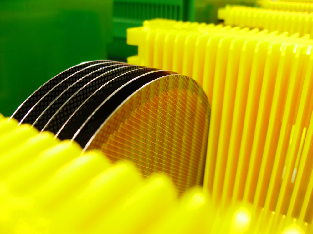
Showa Denko (SDK) has announced that it will increase manufacturing capacity for its high-quality-grade SiC epitaxial wafer for power devices from the current 3,000 to 5,000 wafers per month. Presently on the market under the trade-name High-Grade Epi (HGE), the expanded facility will become operational in April 2018.
Power modules for high-voltage, high-current applications mainly contain devices with the structure of SBD (Schottky Barrier Diode) and transistors with the structure of MOSFET. While manufacturers go into mass production of SiC-SBD, practical application of SiC-MOSFET required further reduction in various types of surface and crystal defects.
In HGE by SDK, the number of basal plane dislocation (BPD), a typical crystal defect, is controlled within 0.1/cm2. Since its release in October 2015, HGE has been used as a key component in SiC-SBD, and is increasingly used by device manufacturers in SiC-MOSFET. SDK is expanding its HGE production capacity as facilities are fully operational at present and we expect a stronger market for SiC-MOSFET in 2018 and beyond.

AngelTech Live III: Join us on 12 April 2021!
AngelTech Live III will be broadcast on 12 April 2021, 10am BST, rebroadcast on 14 April (10am CTT) and 16 April (10am PST) and will feature online versions of the market-leading physical events: CS International and PIC International PLUS a brand new Silicon Semiconductor International Track!
Thanks to the great diversity of the semiconductor industry, we are always chasing new markets and developing a range of exciting technologies.
2021 is no different. Over the last few months interest in deep-UV LEDs has rocketed, due to its capability to disinfect and sanitise areas and combat Covid-19. We shall consider a roadmap for this device, along with technologies for boosting its output.
We shall also look at microLEDs, a display with many wonderful attributes, identifying processes for handling the mass transfer of tiny emitters that hold the key to commercialisation of this technology.
We shall also discuss electrification of transportation, underpinned by wide bandgap power electronics and supported by blue lasers that are ideal for processing copper.
Additional areas we will cover include the development of GaN ICs, to improve the reach of power electronics; the great strides that have been made with gallium oxide; and a look at new materials, such as cubic GaN and AlScN.
Having attracted 1500 delegates over the last 2 online summits, the 3rd event promises to be even bigger and better – with 3 interactive sessions over 1 day and will once again prove to be a key event across the semiconductor and photonic integrated circuits calendar.
So make sure you sign up today and discover the latest cutting edge developments across the compound semiconductor and integrated photonics value chain.
REGISTER FOR FREE
VIEW SESSIONS