
Semiconductor supermirrors
Advancing precision laser optics with substrate-transferred epitaxial films
BY GARRETT COLE, MARK WHITE, MARKUS ASPELMEYER AND CHRISTIAN PAWLU FROM CRYSTALLINE MIRROR SOLUTIONS
Multilayer optical interference coatings are everywhere. They are employed in consumer products, including anti-reflection coatings in spectacles, cameras, binoculars, consumer electronics, and residential and commercial lighting; they are in industry, in lasers, inertial navigation systems, and tools for lithography and wafer inspection; and they are in scientific labs, in the mirrors, beam-splitters, and polarizers found in fundamental experiments, such as the detection of gravitational waves.
All of these coatings are essentially alternating layers of high and low refractive index materials that provide wavelength selective reflectance "“ and as you'd expect, you get what you pay for. At the lower end are coatings formed through the evaporation of metals and dielectric films, and at the other extreme are ultra-low-loss coatings formed from high-density sputtering of amorphous multilayers. In total, this optical coatings industry is worth billions of dollars.
The current "˜gold standard' for the optical interference coating is the ion-beam sputtered multilayer. Primarily, it consists of alternating layers of amorphous metal oxides "“ most commonly the pairing of high-index Ta2O5 and low-index SiO2. So long as there is reasonable adhesion with the base substrate, the sputtered films can be coated on nearly any surface, even those that are patterned.
One of the strengths of this technology, originally developed for the construction of ring-laser gyroscopes, is the very low levels of optical scatter and absorption loss. The loss levels are so low that they are measured in the parts per million. It is a level of performance that has enabled ion-beam sputtering to be firmly established as the prime technology for generating ultra-low-loss reflectors in the visible and near-infrared.
In general, such interference coatings have little overlap with the compound semiconductor industry. But there is one key exception: the VCSEL. This class of laser diode features a multi-quantum-well active region sandwiched between two epitaxial mirrors, typically referred to as distributed Bragg reflectors, which consist of alternating layers of high and low refractive index semiconductors.

Figure 1: Ion beam sputtering (IBS) is used to deposit low-loss multilayers of amorphous metal oxides. In this case, a beam of ionized noble gas atoms impinges on a metallic target and, reacting with an oxidizing chamber environment, is directly deposited on an optical substrate.
A distinct disadvantage of defect-free epitaxial multilayers, compared with sputtered films, is their need for substrate lattice matching. The growth of these single-crystal epilayers must proceed on a planar surface with a nearly identical inter-atomic spacing, as well as a matched crystalline symmetry. Due to this stringent constraint, substrate options for direct crystal growth are severely limited. Consequently, while ion-beam sputtering has been used to make many high-end coatings in a wide variety of general optics applications, compound semiconductor interference coatings, such as distributed Bragg reflectors based on the pairing of GaAs and AlGaAs, have, so far, been confined to the domain of surface-normal optoelectronics.
At Crystalline Mirror Solutions, a spin-off of the University of Vienna, we have overcome this limitation. Our team, based in Santa Barbara, CA, and Vienna, Austria, (with in-house epitaxial capabilities in Zurich, Switzerland) has developed the expertise to extract and transfer epitaxial multilayers from their native growth wafers to bulk optical substrates, so they can compete head-to-head with direct deposited amorphous coatings.
Our structures combine exceptional optical performance with a number of unique and advantageous physical properties that are enabled through the use of compound semiconductor materials. These include a high mechanical quality factor for minimising Brownian noise, a wide transparency window from roughly 900 nm to 10 µm enabling very low-loss mirrors to be realized in both the near- and mid-infrared spectral region, and a superior thermal conductivity "“ at least an order-of-magnitude higher than that for traditional sputtered films.
Fabrication of our mirrors is based on substrate-transfer and direct bonding, and draws on traditional semiconductor processes, such as epitaxial growth, lithography, and various wet and dry etching techniques. Production begins with the growth of epilayers by MBE, which is chosen for its capability to realise materials of exceptional purity. This high purity leads to very low levels of background doping and absorption, properties that yield ultra-high reflectivity supermirrors. Fabrication is completed by removing the single-crystal multilayer from the original growth wafer and transferring it to the final optic, using post-growth wet and dry etching.

Figure 2: A brief timeline of optical coating techniques, highlighting the approximate development dates for various processes. Crystalline coatings represent a significant departure from all previous techniques involving amorphous or poly-crystalline materials, in that the constituent materials of the coating are single-crystalline materials.
One of the strengths of our pioneering technology is that it allows the direct bonding of epitaxial coatings to curved surfaces. Currently, the radius of curvature can be as tight as 10 cm.
The majority of our work involves coating fused silica substrates and producing near-infrared optics with a centre wavelength between 1000 nm and 2000 nm. However, we have realized high-quality crystalline coatings on a wide variety of substrates, including silicon, sapphire, SiC, diamond, YAG, and YVO4. The maximum coating area for a continuous structure is limited to the size of the original growth wafer, so we are able to offer material with dimensions up to 20 cm in diameter.
With prototype coatings fabricated in 2012, we first published the results of our process in 2013 in a joint paper with Jun Ye's group at JILA in Boulder, CO (reference included in the caption of Figure 4 below). Following four years of refinement, our substrate-transferred crystalline coatings have now emerged as an alternative high-performance option for optical interference coatings in demanding optics applications.

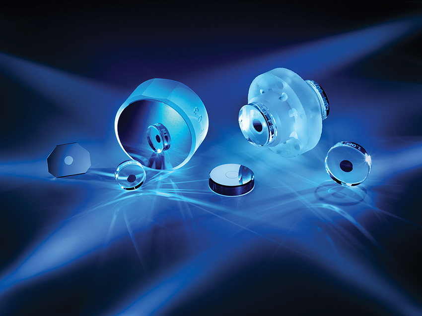
Figure 3: A typical semiconductor supermirror consists of a fused silica optical substrate and a direct-bonded crystalline coating. The 8 mm-diameter coating disc consists of an alternating stack of high-refractive-index GaAs and low-index Al0.92Ga0.08As layers. Following a lithographic process to define and etch the lateral geometry of the coating, the epitaxial film stack is removed from the growth wafer and fused to the final optic, in this case a 25.4 mm-diameter by 6.35 mm-thick fused silica substrate, with a 0.5 m-radius of curvature.
Our coatings in the near-infrared, for centre wavelengths spanning 1064 nm to 1560 nm, have an excess optical loss "“ given by summing scatter and absorption "“ of less than 5 parts per million. Assuming a finite optical transmission, the reflectivity of such a mirror is 0.999992, and the cavity finesse is up to 400,000 at the telecom-relevant wavelength range near 1550 nm. This level of optical performance is fully on par with that of high-quality, ion-beam sputtered films, and it confirms that an optimized MBE process can produce films that combine extremely high purity with high surface quality. However, one aspect that is typically overlooked in the development of precision optical components is the material's mechanical quality factor, Q "“ this quantity is the inverse of the mechanical dissipation, or imaginary component of the Young's modulus. For some advanced systems, such as precision interferometers utilized for the measurement of gravitational waves and stabilizing reference cavities for optical atomic clocks, it is Q that governs the ultimate stability of the system and sets the noise floor for unwanted thermo-mechanical fluctuations of the object.
There will always be some movement of any optical element, because constituent atoms will fluctuate in position due to random Brownian motion. However, the magnitude of this random motion, and thus the limiting noise in terms of displacement sensitivity, will depend strongly on the mechanical Q of the constituent materials of the system. The performance of today's precision optical interferometers is so high that this ultimate thermal noise limit is now becoming a significant impediment to further improvement.
The good news is that a switch from existing, high-performance optical coatings to our semiconductor supermirrors can improve the mechanical Q by a factor of 10 to 100. It is this immediate reduction in mechanical loss and resulting reduction in Brownian thermal noise that provided the original impetus for developing our technology, and is now a driving force for its refinement.
Over the last few years we have manufactured and delivered optics that are being used in the construction of the world's most stable laser systems, which are located in various international metrology laboratories. This includes: room temperature and cryogenic reference cavities for lasers operating at telecom-relevant wavelengths near 1550 nm; dedicated systems targeting clock transition wavelengths for trapped aluminium-ion clocks, as well as neutral atom lattice clock systems based on strontium and ytterbium; and prototype optics for exploring performance improvements that may be possible with crystalline coatings in gravitational wave astronomy.
During the years that follow, our coatings should lead to advances in optical interferometers for precision metrology, with one highlight being the significant improvement in clock performance that can be realized with the roll-out of mHz-linewidth laser systems.

Figure 4: Demonstration of the significant reduction in mechanical damping and thus the limiting coating thermal noise for substrate-transferred crystalline coatings. At 1 Hz the AlGaAs crystalline coating yields a ten-fold improvement in Brownian noise over traditional ion beam sputtered coatings based on SiO2/Ta2O5 multilayers. This plot is reproduced from G. D. Cole, W. Zhang, M. J. Martin, J. Ye, M. Aspelmeyer, "Tenfold reduction of Brownian noise in high-reflectivity optical coatings," Nature Photonics 7 644, August 2013.
Mid-infrared possibilities
Another attribute of our epitaxial multilayer structure is its exceptionally high optical transparency over a wide spectral range. With this GaAs-based material system, low optical losses can be maintained over a range that extends from approximately 900 nm to 10 µm "“ and potentially beyond. In contrast, amorphous metal oxides tend to exhibit significant excess absorption beyond 2 µm.
Recent investigations of our semiconductor supermirrors for use in optical sensing in the mid-infrared "“ the centre wavelengths for these mirrors are from 3 µm to 4 µm "“ highlights their exceptional performance. Direct absorption measurements at 3.7 µm reveal limiting losses as low as 5 parts per million. This level of performance opens the door to new scientific discoveries in chemical kinetics, via time-resolved optical frequency comb spectroscopy.
Efforts in this direction include a ground-breaking experiment led by Jun Ye's group at JILA, a joint institute of NIST and the University of Colorado Boulder. Using an experimental set-up that included our mirrors, these researchers delivered a breakthrough in the understanding of combustion by unlocking the fundamental reaction kinetics of the deuterated hydroxyl molecule, OD, and carbon monoxide. Under thermal reaction conditions, Ye and co-workers observed, for the first time, trans-DOCO (the deuterated analogue of the trans- hydrocarboxyl radical). This elusive, short-lived intermediate compound is crucial for processes relevant to earth and planetary sciences, and the burning of fossil fuels.
We believe that this type of mirror can be further improved, leading to an optical loss at the parts-per-million level in this difficult wavelength window. Our superlattice stacks can be transferred to a variety of mid-IR compatible substrates, including single-crystal silicon, zinc selenide, calcium fluoride, germanium, and GaAs.
Superior conductivity
Opportunities for our mirrors exist in high-power laser systems for materials processing. These systems require optics with minimal thermal distortion and excellent thermal conductivity "“ criteria that our mirrors excel in. Compared with the incumbent technology, amorphous metal oxides, our mirrors have a significantly higher thermal conductivity "“ it is typically 30 W m-1K-1 versus 1 W m-1K-1 for low-loss metal oxides.
This virtue, combined with optical absorption levels below parts per million, makes our mirrors an excellent choice for reflectors in demanding laser-processing applications. Here, they should enjoy the greatest success in kilowatt-class CW or quasi-CW laser systems that are employed for cutting, welding and brazing. And if the semiconductor supermirrors have to operate in harsh thermal environments, they can be united with thermally-optimized substrate materials, such as diamond or SiC. This promises to redefine the performance metrics for reflectors operating in these conditions.
While our company and technology may still be quite young, we have already demonstrated that our substrate-transferred, compound-semiconductor-based optical interference coatings can radically enhance performance in critically demanding optics applications. This is due to their tremendous attributes: the lowest mechanical loss, and thus Brownian noise; the highest thermal conductivity; and the widest spectral coverage of any optical coating technology. Looking ahead, there is a bright future for crystalline coatings in applications requiring the ultimate levels of optical, thermal, and optomechanical performance.


