
Substrates & Materials Award
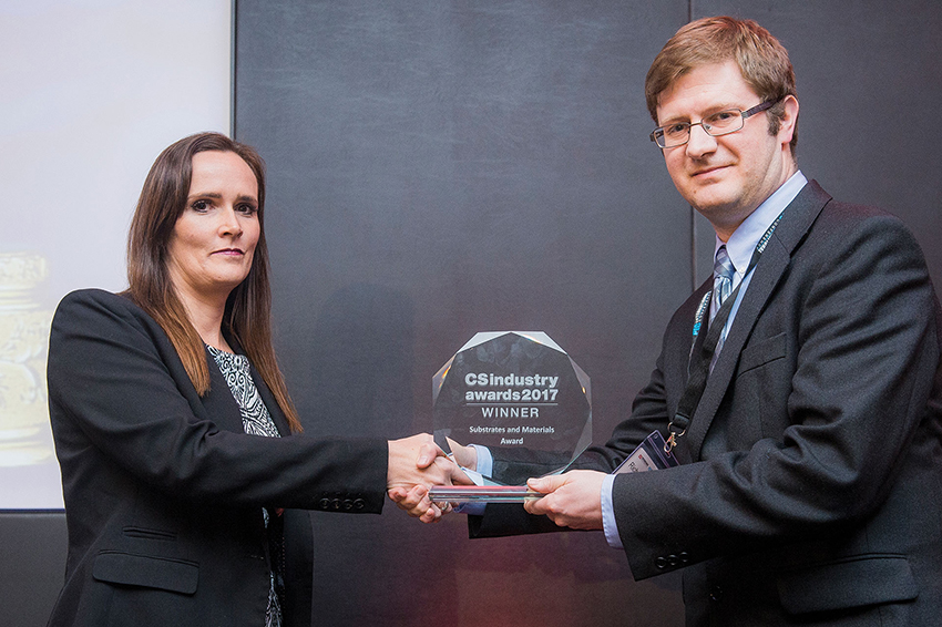
ENTRY: Element Six TM200

Element Six's TM200 is the highest thermal conductivity bulk heat spreader material available in the market with room temperature thermal conductivity >2000 W/mK (more than 5x copper or 10x other commonly used ceramic materials).
Element Six has developed specialized chemical vapor deposition (CVD) processes to produce free standing diamond substrates that deliver this market's leading thermal conductivity. Designed to enable extreme performance thermal packaging for use in high power, or high power density devices, TM200 enables increased power and reliability and reduced system size.
Element Six's TM200 is a top tier grade of CVD diamond thermal material. In achieving the properties discussed previously, as well as extreme isotropy in thermal conductivity (kcrossplane/kinplane~1.0), the synthesis was tuned to satisfy such technical and commercial criteria:
All aspects of transport phenomena, chemistry and electromagnetic affects that can have significant impact on the figures of merit of any CVD diamond process which are: Repeatability of process; Volume growth consistent with cost/performance metrics; Thickness uniformity; Process stability to achieve a total of diamond thickness greater than 3 mm; High average bulk thermal conductivity (Quality of growth); Scalability, meaning each stage can in principal be reproduced, measured and controlled while the increasing the throughput and/or growth area, Consistent nucleation and seeding methodology.
Synthesizing CVD diamond covers only half the engineering technology to manufacture the TM200. Post-synthesis processing covers the other half. Through novel techniques and advanced engineering practices, Element Six fabricates the TM200 with exceptional dimensional tolerances, for instance specifications: Planar dimensional tolerance = -0.0/+0.1mm; Thickness tolerance = ±0.050 mm; Polished Surfaces: Ra < 10 nm; No more than ± 10 nm variation of Ra (over 25 mm diameter); Flatness < 0.010 mm (over 25 mm diameter)
All the above has been incorporated in a platform that delivers more than 2000 W/mK thermal conductivity with 1012 Ω-cm bulk and 1010 Ω-cm surface resistivity; a truly great feat in engineering product development. This advanced grade of CVD diamond thermal material offers developers of high power, or high power density devices a thermal solution which can successfully operate within extreme performance environments. The TM200's combination of properties, such as high thermal conductivity, electrical insulation, low density and chemical inertness has been designed specifically for advanced thermal management packaging applications.


