EpiGaN to Supply OMMIC with GaN/Si Material

Partnership on GaN/Si epi wafers will target RF power products fort future 5G wireless communication
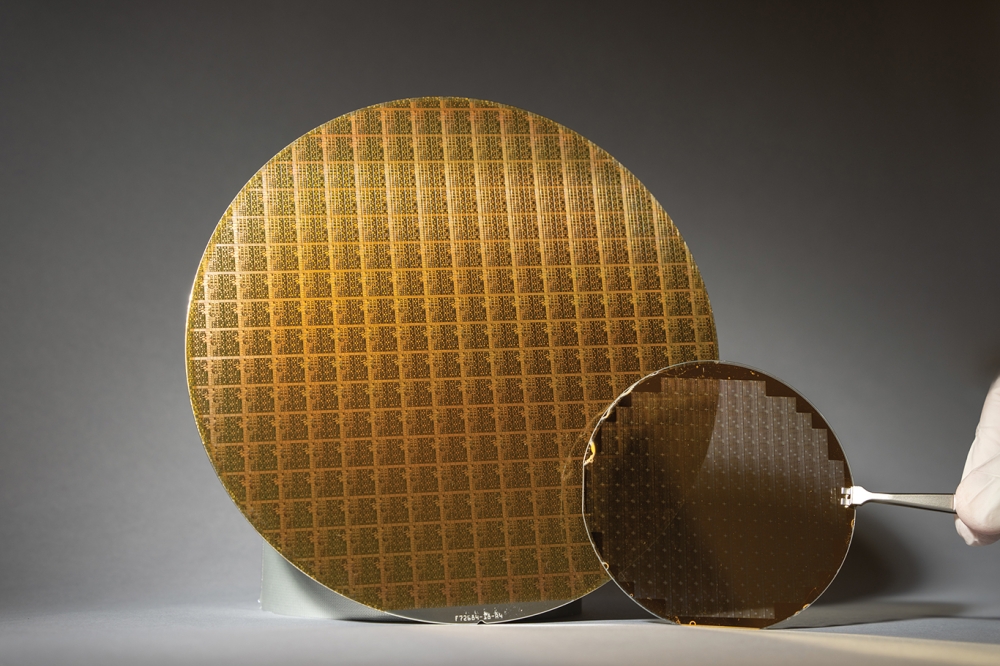
Following the recent inauguration of Europe's first 150mm GaN production line at OMMIC's site in Limeil-Brévannes near Paris, EpiGaN and OMMIC have announced a partnership on GaN/Si epiwafers supply for RF power products aiming at future 5G wireless communication.
EpiGaN, a supplier of GaN-on-Si and GaN-on-SiC material solutions for advanced electronic products, and OMMIC, a provider of compound semiconductor MMICs and foundry services, are collaborating in the development of RF GaN/Si technology on 150-mm diameter wafers. They have jointly collaborated on establishing a production process based on EpiGaN's differentiating GaN/Si material technology with in-situ grown SiN passivation.
They will cooperate directly to move this technology to 150-mm diameter wafers, targeting future 5G wireless communication standards, for which OMMIC last week announced a large project with a 5G equipment supplier.
"EpiGaN is honoured to team up with OMMIC for scaling up to a 150-mm GaN/Si process line based on EpiGaN's differentiating technology addressing products for 5G," commented EpiGaN CEO Marianne Germain. "We offer many attractive USPs for RF power, which add value to device designers, such as in-situ SiN passivation for enhanced device robustness, or very low RF losses up to 100GHz. We are proud of the high-frequency capability of our material, which enables a very cost-efficient and energy-efficient GaN technology for the higher frequency bands targeted by 5G."
"The next-generation 5G standard will require GaN as an enabling semiconductor technology to provide a step-up in performance," stated OMMIC CEO Marc Rocchi. "Only then will the experience for the end user be superb. Teaming up with EpiGaN is an essential element of our growth strategy and it enables us to meet the required volume and quality levels for our 5G GaN MMICs."
EpiGaN is using its expertise in GaN technology to manufacture GaN material at the production site in Hasselt, Belgium. EpiGaN's HVRF power structures are available on both SiC (up to 150mm) and Si substrates (up to 200mm). They offer high power densities for mm-wave bands combined with lowest RF losses (<0.5dB/mm up to 50GHz, <1dB/mm up to 100 GHz). An additional advantage of EpiGaN's wafer technology is the in-situ SiN capping layer. This provides superior surface passivation and the use of pure, ultra-thin AlN layers as barrier materials results in superior mmW performance, reducing short-channel transistor effects.
Headquartered in Limeil-Brévannes, France, OMMIC was founded in 2000 as a spinout from Philips Microwave Limeil (PML). OMMIC is a supplier of MMIC circuits, foundry services and of Eepitaxial wafers based on III-V (GaAs, GaN and InP) materials. The design and manufacturing facilities of OMMIC are based near Paris, France. Technologies include mixed mode E/D PHEMT, Low Noise and Power PHEMT, metamorphic HEMT and InP DHBT allowing the design of a wide range of MMICs including LNAs from 900 MHz to 160 GHz, Highly Integrated T/R Functions and Millimeter wave power amplifiers


