
Lasertec announces GaN Wafer Inspection tool
GALOIS Series uses bright-field confocal optics, enabling high-speed inspection of various kinds of GaN wafer defects and high-resolution observation of defect images
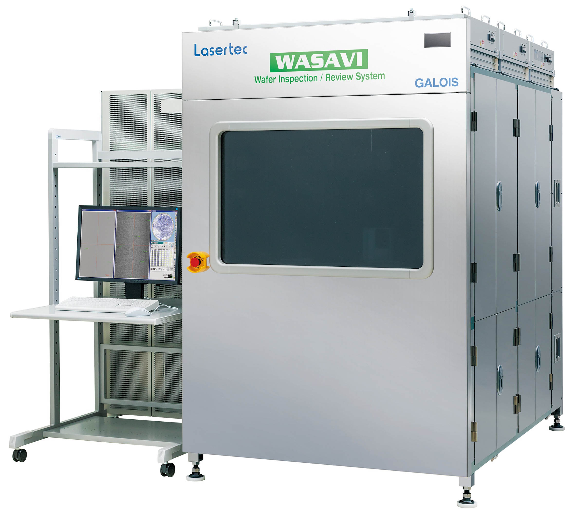
Lasertec has launched a new defect inspection and review system series named GALOIS, which is designed specifically for the inspection and analysis of GaN wafers. It is already accepting orders.
The GALOIS Series uses bright-field confocal optics, enabling high-speed inspection of various kinds of GaN wafer defects and high-resolution observation of defect images.
Lasertec says its SICA88 is widely used as SiC inspection tool, enjoying strong market recognition due to its high throughput, high accuracy of defect classification, high-resolution defect review, and more. GaN, on the other hand, lags behind in device usage, hindered by the high cost of GaN wafer manufacturing and the presence of numerous crystallographic and process defects in wafers, requiring further efforts in wafer quality improvement.
The Lasertec GALOIS Series, which offers the high-speed, high-sensitivity detection and classification of crystallographic and process defects, combined with high-resolution defect image review, has been launched to assist these efforts. GALOIS uses a combination of confocal optics and differential interferometry optics "“ both of which are Lasertec core technologies "“ with a sophisticated algorithm based on advanced imaging technology.
This eliminates the effect of noise from the backside of a transparent substrate, or from surface morphology, enabling the high-sensitivity detection of various kinds of defects in GaN wafers.
GALOIS employs a high-speed processing computer system and a model based on machine learning, including advanced Deep Learning, for defect classification. GALOIS uses the highresolution review images captured by the above mentioned Lasertec core technologies and accurately classifies indeterminately formed defects, in parallel with other inspection processing. All review images captured during inspection of whole wafers are saved to computer storage, and can be utilized for analysis of unclassified defects.
GALOIS achieves an inspection speed of 6 minutes per 6-inch wafer, which is fast enough for future application in the production phase. In addition to being an outgoing and incoming inspection tool for GaN wafers, GALIOS also takes the role of a strong process and yield improvement tool. It helps in identifying the root cause of defects, acting as a wafer, epitaxy, and device process monitor.


