
KAUST team makes see-through circuits
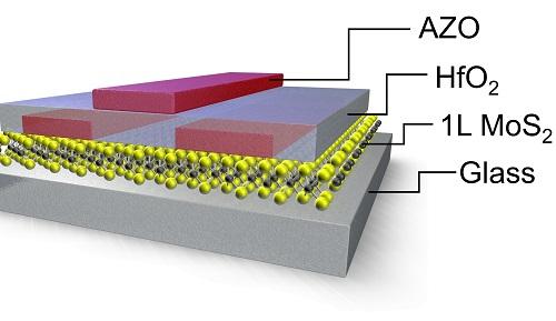
Researchers have made a fully transparent thin-film transistor consisting of a MoS2 monolayer; HfO2, which is used for coating; and aluminum-doped zinc oxide (AZO) contacts
See-through electronic devices, such as transparent displays, smart windows and concealed circuits require completely translucent components if users are to digitally interact with their perceived surroundings and manipulate information in real time. Now, researchers from KAUST (King Abdullah University of Science and Technology) have devised a way to integrate transparent conducting metal-oxide contacts with 2D semiconductors such as MoS2 into these devices.
Ultrathin sheets of transition metal chalcogenide-based 2D semiconductors such as 2D MoS2, present exceptional electronic properties and optical transparency. However, to date, incorporating MoS2 monolayers into circuits has relied on silicon substrates and metal electrodes, such as gold and aluminum. The opacity of these materials has stalled attempts to develop fully transparent 2D electronic devices.
The KAUST team led by material scientists Xi-Xiang Zhang and Husam Alshareef has combined MoS2 monolayers with transparent contacts to generate a series of devices and circuits, such as transistors, inverters, rectifiers and sensors. The contacts consisted of aluminum-doped zinc oxide (AZO), a low-cost transparent and electrically conductive material that may soon replace the widely used indium-tin oxide. "We wanted to capitalise on the excellent electronic properties of 2D materials, while retaining full transparency in the circuits," explains Alshareef.
Pictured above is a fully transparent thin-film transistor consisting of a MoS2 monolayer; HfO2 which is used for coating; and aluminum-doped zinc oxide (AZO) contacts
According to Alshareef, the researchers grew the contacts over a large area by atomic-layer deposition, during which individual atom layers precisely accumulate on a substrate. Their main difficulty was to also form high-quality MoS2 monolayers on silicon-based substrates over a large area. "We overcame this by using an interfacial layer that promotes MoS2 growth," says Alshareef.
The team also developed a water-based transfer process that moves the as-deposited large-area monolayers onto a different substrate, such as glass or plastic. The researchers then deposited the AZO contacts on the transferred 2D sheets before manufacturing the devices and circuits.
The resulting devices outperformed their equivalents equipped with opaque metal contacts, such as gate, source and drain electrodes, which demonstrates the high compatibility between transparent conducting metal-oxide contacts and MoS2 monolayers. "The transistors fabricated by the large-area process showed the lowest turn-on voltage of any reported MoS2 monolayer-based thin-film transistor grown by chemical vapour deposition," says PhD student Zhenwei Wang, first author of the study.
"Additional circuits are planned that will help demonstrate that our approach is robust and scalable" says Alshareef.


