Startup Demonstrates Ultra-High Resolution Micro-LED Micro-Displays
.jpg)
JBD, a Hong Kong based technology startup, reports that its researchers have created the first monochromatic red, green and blue active matrix micro-LED (AMμLED; also referred to as mLED or ILED) micro-displays with greater than 5,000 dpi pixel density by utilizing a wafer scale monolithic hybrid integration process. The company said it believes their AMμLED micro-displays have the highest pixel density of its kind and offer high brightness and contrast ratios at low power consumption and in a small device footprint. The company also claims its technology demonstrates a clear path for mass production of AMμLED micro-displays using existing mature semiconductor infrastructure and processes for emerging applications such as wearable electronics and augmented reality (AR) headsets.
Compared with existing technologies such as LCD and OLED micro-displays, micro-LED micro-displays offer significant performance improvements in brightness/contrast, energy efficiency, response time and reliability. Currently, micro display panels are typically hybrids of micro-LED arrays with CMOS active matrix (AM) driver ICs that utilize flip-chip technology. However, several drawbacks exist in this manufacturing method: first, flip-chip processes typically suffer from low through-put, resulting in higher costs compared with other semiconductor technologies; second, the built-in stress of producing hybrid chips due to thermal mismatch between the LED epi substrate and Si substrate of ICs during the bonding process may lead to manufacturing yield loss and long-term reliability issues. Furthermore, manufacturers have found that the alignment accuracy of bonding equipment can be a limiting factor that makes it difficult to push the pixel pitch down to a few microns, which is highly desired for some applications such as AR, the company stated.
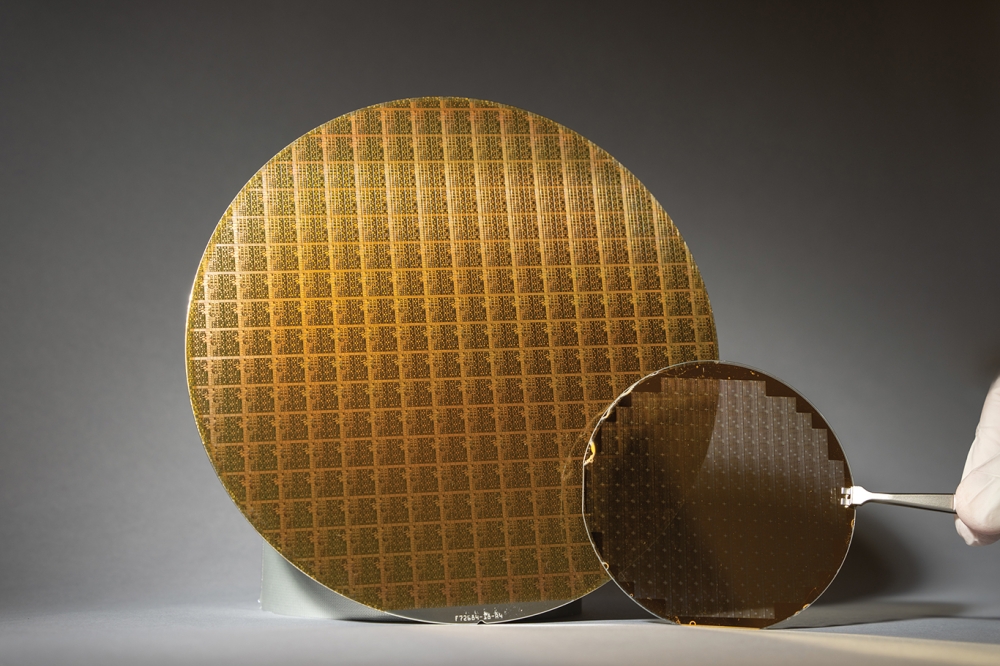
To address those challenges, JBD has developed a new monolithic hybrid integration technology. Through wafer bonding followed by substrate removal processes, JBD said it has successfully transferred the functional compound semiconductor epi layers onto Si IC wafers. Such wafer-level blank epi transfer eliminates the need of precise alignment as required in flip-chip based processes. JBD said its approach provides higher throughput, making it suitable for large volume and low-cost production. JBD's epi-on-IC templates are subsequently subjected to the standard semiconductor fabrication processes with high alignment accuracy to produce monolithic hybrid optoelectronics integrated circuit (OEIC) chips.
Using JBD's monolithic hybrid integration technology, monochromatic red, green and blue micro-LED micro-displays have been successfully demonstrated on Si based active matrix micro-display IC backplanes. The company's AMμLED micro-displays have achieved high resolution with 5μm pixel pitch. The brightness of the AMμLED micro-display (green) in test circuits well exceeds 5x10⁵cd/m2, representing an improvement of over 500-times compared to the existing self-emissive micro-displays. JBD said that it believes with further optimization of the device design and fabrication process, its solution can lead to AMμLED micro-displays with resolution of over 10,000 dpi, which will make it the most desirable and promising solution for various wearable electronics and AR applications.
Details of JBD's work will be presented at SID International Conference on Display Technology (ICDT)
2018 and SID Display Week 2018. For further details, contact Fang Ou at this address: fang_ou@jb-display.com


