
Researchers reveal limits of InGaN quantum wells in LED lighting
New findings answer long-standing question around the efficiencies of InGaN-based green and red LEDs
For the first time an international research group has revealed the core mechanism that limits the indium content in InGaN thin films "“ the key material for blue LEDs.
Increasing the indium content in InGaN quantum wells is the common approach to shift the emission of III-Nitride based LEDs towards the green and, in particular, red part of the optical spectrum, necessary for the modern RGB devices. The new findings answer the long-standing research question: why does this classical approach fail, when we try to obtain efficient InGaN-based green and red LEDs?
Despite the progress in the field of green LEDs and lasers, the researchers could not overcome the limit of 30 percent of indium content in the films. The reason for that was unclear up to now: is it a problem of finding the right growth conditions or rather a fundamental effect that cannot be overcome?
Now, an international team from Germany, Poland and China has shed new light on this question and revealed the mechanism responsible for that limitation.
In their work the scientists tried to push the indium content to the limit by growing single atomic layers of InN on GaN. However, independent of growth conditions, indium concentrations have never exceeded 25 percent to 30 percent "“ a clear sign of a fundamentally limiting mechanism.
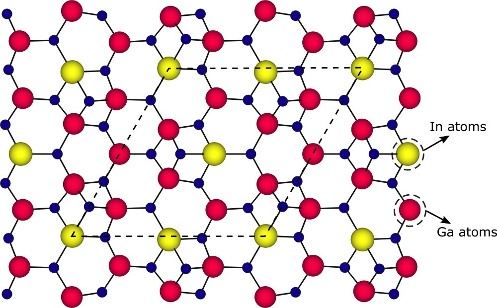
The researchers used advanced characterisation methods, such as atomic resolution transmission electron microscope (TEM) and in-situ reflection high-energy electron diffraction (RHEED), and discovered that, as soon as the indium content reaches around 25 percent, the atoms within the (In, Ga)N monolayer arrange in a regular pattern "“ single atomic column of In alternates with two atomic columns of gallium atoms.
Comprehensive theoretical calculations revealed that the atomic ordering is induced by a particular surface reconstruction (shown above): indium atoms are bonded with four neighbouring atoms, instead of expected three. This creates stronger bonds between indium and nitrogen atoms, which, on one hand, allows to use higher temperatures during the growth and provides material with better quality. On the other hand, the ordering sets the limit of the In content of 25 percent, which cannot be overcome under realistic growth conditions.
"Apparently, a technological bottleneck hampers all the attempts to shift the emission from the green towards the yellow and the red regions of the spectra. Therefore, new original pathways are urgently required to overcome these fundamental limitations", states Tobias Schulz, the researcher from the Leibniz-Institut fuer Kristallzuechtung and one of the authors of the work, "For example, growth of InGaN films on high quality InGaN pseudo-substrates that would reduce the strain in the growing layer."
However, the discovery of ordering may help to overcome well known limitations of the InGaN material system: localisation of charge carriers due to fluctuations in the chemical composition of the alloy. Growing stable ordered (In, Ga)N alloys with the fixed composition at high temperatures could thus improve the optical properties of devices.
The work is a result of a collaboration between Leibniz-Institut fuer Kristallzuechtung (Berlin, Germany), Max-Planck-Institut fuer Eisenforschung (Duesseldorf, Germany), Paul-Drude Institut fuer Festkörperelektronik (Berlin, Germany), Institute of High-Pressure Physics (Warsaw, Poland), and State Key Laboratory of Artificial Microstructure and Mesoscopic Physics (Beijing, China).
'Elastically frustrated rehybridization: Origin of chemical order and compositional limits in InGaN quantum wells' by L. Lymperakis et al; Phys. Rev. Materials 2, 011601(R) "“ Published 8 January 2018


