
AFRL team puts the case for gallium oxide
Ga2O3 could enable the design of better FETs with smaller geometries and superior energy densities
Silicon has long been the go-to material in the world of microelectronics and semiconductor technology. But silicon still faces limitations, particularly with scalability for power applications. Pushing semiconductor technology to its full potential requires smaller designs at higher energy density.
"One of the largest shortcomings in the world of microelectronics is always good use of power: Designers are always looking to reduce excess power consumption and unnecessary heat generation," said Gregg Jessen, principal electronics engineer at the US Air Force Research Laboratory. "Usually, you would do this by scaling the devices. But the technologies in use today are already scaled close to their limits for the operating voltage desired in many applications. They are limited by their critical electric field strength."
Transparent conductive oxides are a key emerging material in semiconductor technology, offering the unlikely combination of conductivity and transparency over the visual spectrum. One conductive oxide in particular has unique properties that allow it to function well in power switching: Ga2O3 or gallium oxide, a material with an incredibly large bandgap.
In their article published this week in Applied Physics Letters, from AIP Publishing, authors Masataka Higashiwaki and Jessen outline a case for producing microelectronics using Ga2O3. The authors focus on FETs, devices that could greatly benefit from Ga2O3's large critical electric field strength - a quality which Jessen said could enable the design of FETs with smaller geometries and aggressive doping profiles that would destroy any other FET material.
The material's flexibility for various applications is due to its broad range of possible conductivities - from highly conductive to very insulating - and high-breakdown-voltage capabilities due to its electric field strength. Consequently, Ga2O3 can be scaled to an extreme degree. Large area Ga2O3 wafers can also be grown from the melt, lowering manufacturing costs.
"The next application for Ga2O3 will be unipolar FETs for power supplies," Jessen said. "Critical field strength is the key metric here, and it results in superior energy density capabilities. The critical field strength of gallium oxide is more than 20 times that of silicon and more than twice that of SiC and GaN."
The authors discuss manufacturing methods for Ga2O3 wafers, the ability to control electron density, and the challenges with hole transport. Their research suggests that unipolar Ga2O3 devices will dominate. Their paper also details Ga2O3 applications in different types of FETs and how the material can be of service in high-voltage, high-power and power-switching applications.
"From a research perspective, Ga2O3 is really exciting," Jessen said. "We are just beginning to understand the full potential of these devices for several applications, and it's a great time to be involved in the field."
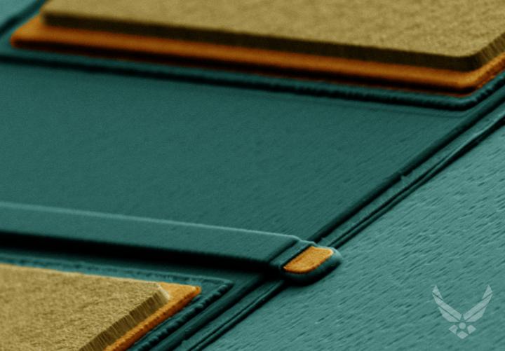
Pictured above: a false-colour, plan-view SEM image of a lateral Ga2O3 FET with an optically defined gate. From near (bottom) to far (top): the source, gate, and drain electrodes. Metal is shown in yellow and orange, dark blue represents dielectric material, and lighter blue denotes the Ga2O3 substrate.


