
2D arsenic sulphide emits light
Scientists demonstrate photoluminescence with a laser excitation wavelength of 473 nm and 632.8 nm
Since the discovery of graphene in 2004, there has been growing interest among scientists in 2D materials 'beyond graphene'. In the family of chalcogenide materials, 2D-layered transition-metal dichalcogenides demonstrate excellent electronic and optical properties, outstanding mechanical flexibility, and exceptional catalytic performance.
At the same time, chalcogenides like As2S3, As2Se3, etc., have never been considered as materials capable of forming structures of this type.
It could be due to the limitations of the methods used for preparing those materials. Now a group of researchers from the laboratory of functional nanomaterials at the Lobachevsky State University of Nizhny Novgorod, the Alekseev Nizhny Novgorod State Technical University and the AGH University of Science and Technology (Krakow, Poland) have shown a way forward.
In their paper 'Infrared and Raman spectroscopy study of As-S chalcogenide films prepared by plasma-enhanced chemical vapor deposition', they demonstrate the possibility of forming honeycomb structural fragments in plasma using the example of the well-known arsenic sulphide chalcogenide system.
They have also shown, for the first time, optical emission of 2D 'beyond graphene' arsenic sulphide prepared in plasma. They produced strong structural photoluminescence exited by continuous wave operation lasers with a laser excitation wavelength of 473 nm and 632.8 nm.
The properties of 2D pole-structured and layered arsenic sulphide are suggested to be the key to advancing to 2D photosensitive devices.
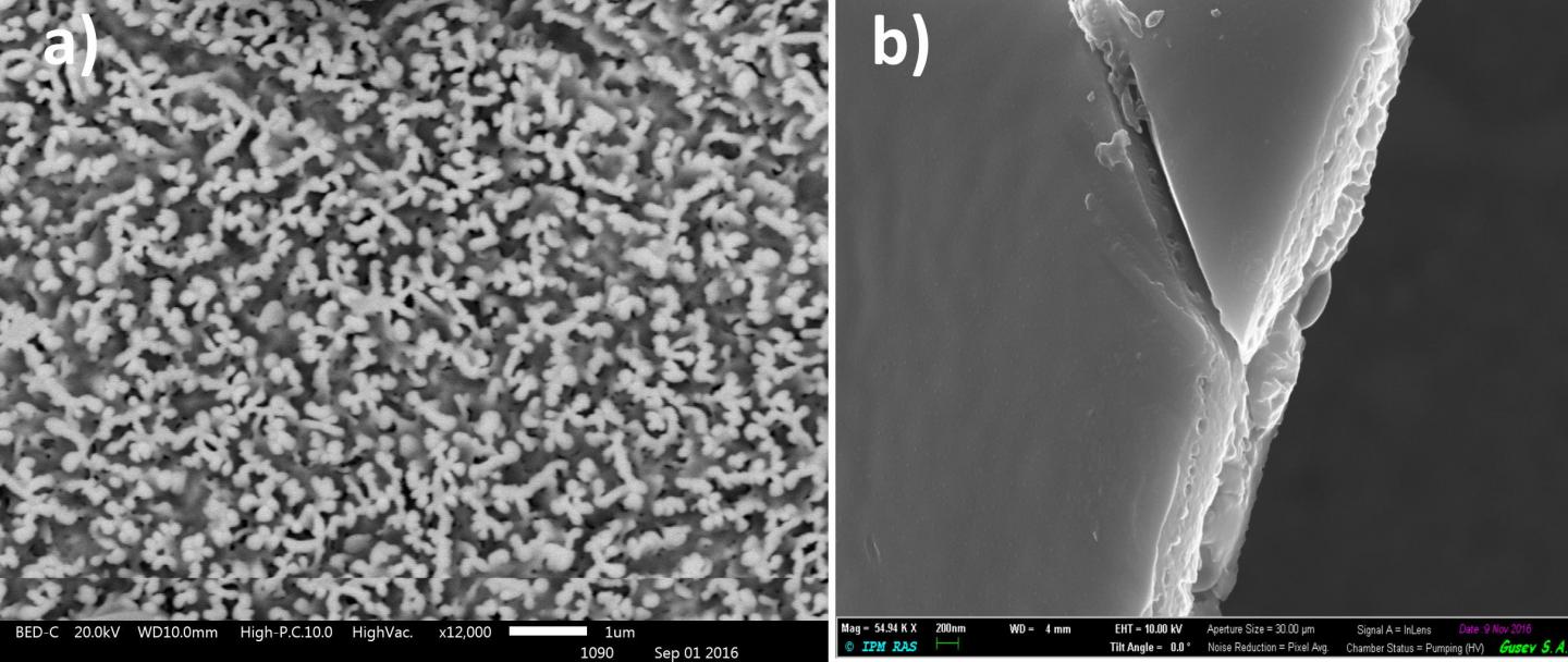
Scanning Electron Microscopy (SEM) images typical of the arsenic sulphide with a composition As40S60 are illustrated in Figure 1 (a) and (b). The striking difference in the surface morphology and structure is due to very different conditions of plasma deposition.
Both pictures (1a and 1b) illustrate arsenic sulphide structures consisting of (As2S3) n-units formed in plasma by spherical structural fragments with a diameter of about 100 nm. Figure 1a shows a pole-structured material and Figure 1b depicts a 2D layered structure, the theoretical possibility of existence of which has been described recently.
Due to its properties, 2D pole-structured and layered arsenic sulphide is a promising material for developing 2D photosensitive devices. These properties are also useful when creating field-effect transistors, highly sensitive photodetectors and gas sensors.
'Infrared and Raman spectroscopy study of As-S chalcogenide films prepared by plasma-enhanced chemical vapor deposition', by Leonid Mochalov et al; Spectrochimica Acta Part A: Molecular and Biomolecular Spectroscopy Volume 193, 15 March 2018, Pages 258-263


