
HBZ team creates novel light-emitting nano-architecture
Growing nanocrystals of GaAs on tiny columns of silicon and germanium could lead to new types of sensors, LEDs, and solar cells
A team at the HZB (Helmoltz Zentrum Berlin) has succeeded in growing nanocrystals of GaAs on tiny columns of silicon and germanium. This enables extremely efficient optoelectronic components for important frequency ranges to be realised on silicon chips.
GaAs semiconductors have better optoelectronic properties compared to silicon. And those properties can be controlled by specific nanostructures. Sebastian Schmitt, Silke Christiansen and their collaborators have succeeded in building such a nanostructure on a silicon wafer covered with a thin, crystalline layer of germanium.
Colleagues from Australia produced the high-quality wafer and sent it to HZB. The thin film of germanium facilitates the growth of GaAs crystals because the lattice constants of germanium and GaAs are almost identical.
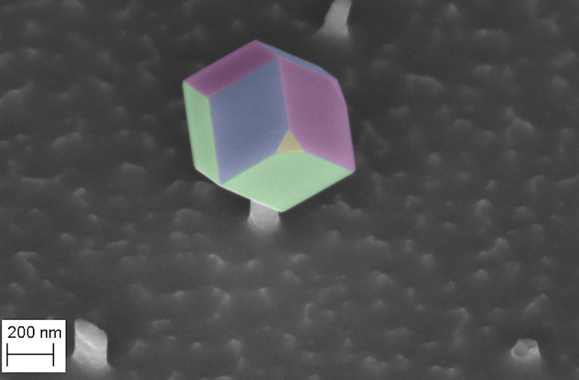
They etched deep trenches in these wafers at intervals of a few micrometers until only a series of fine silicon columns topped with germanium remained on the substrate. GaAs was then deposited using MOVPE.
In this way, both gallium and arsenic atoms were systematically deposited on each germanium-capped silicon tower, forming a tiny, almost-perfect crystal. "The germanium acts like a crystallisation nucleus", explains Schmitt who is the author of the study published in Advanced Optical Materials.
"The nano-architecture looks spectacular under the electron microscope. At first glance, it seems as if you can see a cube on the tip of each silicon needle. At second glance, it becomes apparent that it is actually a rhombic dodecahedron "“ with each of the twelve surfaces an identical rhombus."
This nano-structure exhibits unusually high optical emission after excitation with a laser, especially in the near-infrared region.
"As the GaAs crystals grow, germanium atoms also become incorporated into the crystal lattice", explains Schmitt.
This incorporation of germanium leads to additional discrete energy levels for charge carriers that emit light when falling back to their original levels. The light is then amplified by means of optical resonances in the highly symmetrical nanocrystal, and the frequency of these resonances can be controlled by size and geometry of the crystals. A large number of these so-called photonic resonances could be detected in the experiment that also agree well with numerical calculations.
"Because the optical and electronic properties of semiconductors can be strongly modified by nanostructuring, such nano-architectures are well suited for developing novel sensors, light-emitting diodes, and solar cells", says Schmitt.
'Germanium template assisted integration of GaAs nanocrystals on silicon: a versatile platform for modern optoelectronic material', by S. W. Schmitt et al; Advanced Optical Materials (2018)


