
Fine-tuning 2D MoS2
Penn State team discover why synthetic 2D materials often perform orders of magnitude worse than predicted
A new understanding of why synthetic 2D materials often perform orders of magnitude worse than predicted was reached by teams of researchers led by Penn State. They searched for ways to improve these materials' performance in future electronics, photonics, and memory storage applications.
Researchers make 2D materials using exfoliation - peeling a slice of material off a larger bulk material - or by condensing a gas precursor onto a substrate. The former method provides higher quality materials, but is not useful for making devices. The second method is well established in industrial applications, but yields low performance 2D films.
The researchers demonstrated, for the first time, why the quality of 2D materials grown by the chemical vapour deposition method have poor performance compared to their theoretical predictions. They report their results in a recent issue of Scientific Reports.
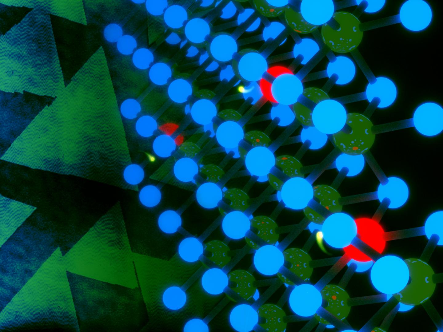
"We grew molybdenum MoS2, a very promising 2D material, on a sapphire substrate," said Kehao Zhang, a doctoral candidate of Joshua Robinson, associate professor of materials science and engineering, Penn State.
"Sapphire itself is aluminum oxide. When the aluminum is the top layer of the substrate, it likes to give up its electrons to the film. This heavy negative doping - electrons have negative charge - limits both the intensity and carrier lifetime for photoluminescence, two important properties for all optoelectronic applications, such as photovoltaics and photosensors."
Once they determined that the aluminum was giving up electrons to the film, they used a sapphire substrate that was cut in such a way as to expose the oxygen rather than the aluminum on the surface. This enhanced the photoluminescence intensity and the carrier lifetime by 100 times.
In related work, a second team of researchers led by the same Penn State group used doping engineering that substitutes foreign atoms into the crystal lattice of the film in order to change or improve the properties of the material. They reported their work this week in Advanced Functional Materials.
"People have tried substitution doping before, but because the interaction of the sapphire substrate screened the effects of the doping, they couldn't deconvolute the impact of the doping," said Zhang, who was also the lead author on the second paper.
Using the oxygen-terminated substrate surface from the first paper, the team removed the screening effect from the substrate and doped the MoS2 2D film with rhenium atoms.
"We deconvoluted the rhenium doping effects on the material," said Zhang. "With this substrate we can go as high as 1 atomic percent, the highest doping concentration ever reported. An unexpected benefit is that doping the rhenium into the lattice passivates 25 percent of the sulphur vacancies, and sulphur vacancies are a long-standing problem with 2D materials."
The doping solves two problems: It makes the material more conductive for applications like transistors and sensors, and at the same time improves the quality of the materials by passivating the defects called sulphur vacancies. The team predicts that higher rhenium doping could completely eliminate the effects of sulphur vacancies.
'Deconvoluting the Photonic and Electronic Response of 2D Materials: The Case of MoS2' by K. Zhang et al: Scientific Reports 7
'Tuning the Electronic and Photonic Properties of Monolayer MoS2 via In Situ Resubstitutional Doping' by K. Zhang et al; Advanced Functional Materials.


