Loading...
News Article

GaNFast chip is at the heart of smallest charger

News

Navitas announces mobile adapter design with five times greater power and twice the power density of standard chargers

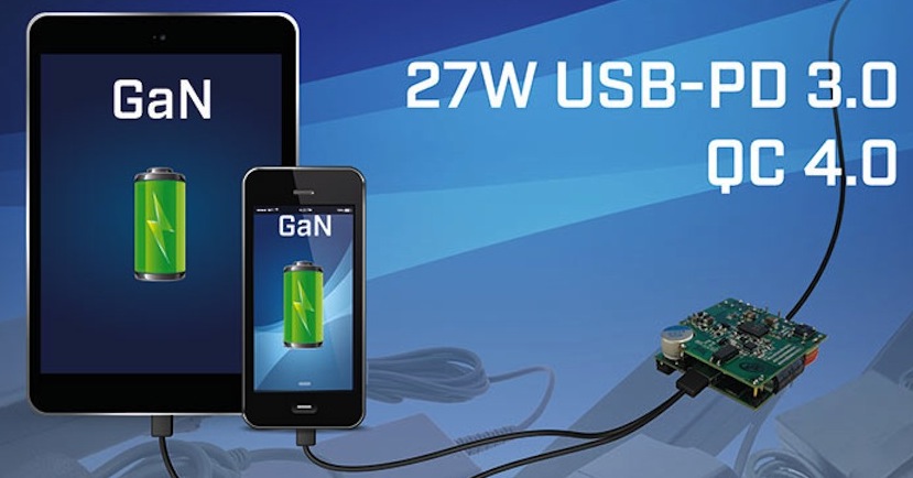
Navitas Semiconductor has announced what is believes is the world's smallest, fastest charging mobile adapter enabled by GaNFast power ICs.

The 27W design delivers five times greater power than standard smartphone chargers and is twice the power density, according to the company.

The lightweight reference design has world-wide input voltage capability and a new Type C connector with USB-PD 3.0 and Qualcomm Quick Charge 4.0 features.

"The 27W is another size and speed breakthrough for consumers enabled by GaNFast technology, and with Quick Charge 4.0 compliance, you can decrease the amount of time you spend tethered to an outlet giving your device "˜five for five' - that's five hours of battery life from five minutes of charging" said Stephen Oliver, Navitas' vice president of sales and marketing.

"Now that the high-frequency power eco-system of GaNFast power ICs, new controllers, new magnetics and soft-switching topologies has been established, we'll see a wide-range of fast-charging, high density designs on the market."

Using a Navitas' high-speed, half-bridge GaNFast power IC in the advanced Active Clamp Flyback (ACF) topology, the 27W reference design measures 39 x 37 x 16 mm (uncased) and achieves a power density of 1.2 W/cm3 (19 W/in3) uncased and 0.7 W/cm3 (11 W/in3) assuming a 2.5mm case thickness.

The 27W design (NVE039) will debut at the Applied Power Electronics Conference (APEC) March 5th in San Antonio, Texas.

Say hello to the heterogeneous revolution
Double heterostructure HEMTs for handsets
AlixLabs to collaborate with Linköping University
SiC MOSFETs: Understanding the benefits of plasma nitridation
Wolfspeed reports Q2 results
VueReal secures $40.5m to scale MicroSolid printing
Mitsubishi joins Horizon Europe's FLAGCHIP project
Vishay launches new high voltage SiC diodes
UK team leads diamond-FET breakthrough
GaN adoption at tipping point, says Infineon
BluGlass files tuneable GaN laser patents
QD company Quantum Science expands into new facility
Innoscience files lawsuit against Infineon
Riber revenues up 5% to €41.2m
Forvia Hella to use CoolSiC for next generation charging
Photon Design to exhibit QD simulation tool
Ortel transfers CW laser fabrication to Canada
Luminus adds red and blue multi-mode Lasers
PseudolithIC raises $6M for heterogeneous chiplet tech
Mesa sidewall design improves HV DUV LEDs
IQE revenue to exceed expectations
'Game-changing' VCSEL system targets clinical imaging
German start-up secures finance for SiC processing tech
Macom signs preliminaries for CHIPS Act funding
IQE and Quintessent partner on QD lasers for AI
EU funds perovskite tandems for fuel-free space propulsion
EU to invest €3m in GeSi quantum project
Transforming the current density of AlN Schottky barrier diodes
Turbocharging the GaN MOSFET with a HfO₂ gate
Wolfspeed launches Gen 4 SiC MOSFET technology
Report predicts high growth for UK's North East
Element Six unveils Cu-diamond composite
×
Search the news archive

To close this popup you can press escape or click the close icon.
Logo
x
Logo
×
Register - Step 1

You may choose to subscribe to the Compound Semiconductor Magazine, the Compound Semiconductor Newsletter, or both. You may also request additional information if required, before submitting your application.


Please subscribe me to:


You chose the industry type of "Other"

Please enter the industry that you work in: