
UCLA researchers show new way to build 2D materials
Electrochemical intercalation method can build artificial 'superlattices' of tens, hundreds or even thousands of layers of 2D materials such as graphene, MoS2 and WSe2 with radically different structures, properties and functions
A research team led by UCLA scientists and engineers has developed a method to make new kinds of artificial 'superlattices' comprising of tens, hundreds or even thousands of alternating layers of ultra-thin 2D materials such as grapheme and MoS2 with radically different structures, properties and functions.
For example, while one layer of this new kind of superlattice can allow a fast flow of electrons through it, the other type of layer can act as an insulator. This design confines the electronic and optical properties to single active layers, and prevents them from interfering with other insulating layers.
Applications include superfast and ultra-efficient semiconductors for transistors in computers and smart devices, and advanced LEDs and lasers.
The study, published in Nature, was led by Xiangfeng Duan, UCLA professor of chemistry and biochemistry, and Yu Huang, UCLA professor of materials science and engineering at the UCLA Samueli School of Engineering.
"Traditional semiconductor superlattices can usually only be made from materials with highly similar lattice symmetry, normally with rather similar electronic structures," Huang said.
"For the first time, we have created stable superlattice structures with radically different layers, yet nearly perfect atomic-molecular arrangements within each layer. This new class of superlattice structures has tailorable electronic properties for potential technological applications and further scientific studies."
One current method to build a superlattice is to manually stack the ultrathin layers one on top of the other. But this is labour-intensive. The other method is to grow one new layer on top of the other, using CVD. But since that means different conditions, such as heat, pressure or chemical environments, are needed to grow each layer, the process could result in altering or breaking the layer underneath. This method is also labor-intensive with low yield rates.
The new method uses electrochemical intercalation, in which a negative voltage is applied. This injects negatively charged electrons into the 2D material. Then, this attracts positively charged ammonium molecules into the spaces between the atomic layers. Those ammonium molecules automatically assemble into new layers in the ordered crystal structure, creating a superlattice.
"Think of a two-dimensional material as a stack of playing cards," Duan said. "Then imagine that we can cause a large pile of nearby plastic beads to insert themselves, in perfect order, sandwiching between each card. That's the analogous idea, but with a crystal of 2D material and ammonium molecules."
The researchers first demonstrated the new technique using black phosphorus as a base 2D atomic crystal material. Using the negative voltage, positively charged ammonium ions were attracted into the base material, and inserted themselves between the layered atomic phosphorous sheets."
Following that success, the team inserted different types of ammonium molecules with various sizes and symmetries into a series of 2D materials including MoS2 and WSe2 to create a broad class of superlattices. They found that they could tailor the structures of the resulting monolayer atomic crystal molecular superlattices, which had a diverse range of desirable electronic and optical properties."The resulting materials could be useful for making faster transistors that consume less power, or for creating efficient light-emitting devices," Duan said.
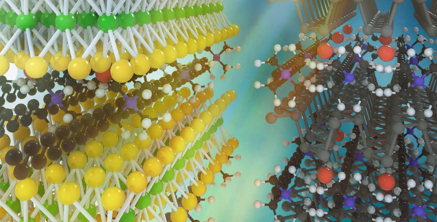
(The picture at the top is an artist's concept of two kinds of monolayer atomic crystal molecular superlattices. On the left, MoS2 with layers of ammonium molecules, on the right, black phosphorus with layers of ammonium molecules.)
'Monolayer atomic crystal molecular superlattices' by Chen Wang et al: Nature volume 555, pages 231"“236 (08 March 2018)


