
Scientists show new way to gauge nanowire growth
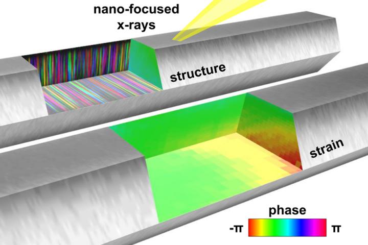
Bragg ptychography approach allows Argonne researchers to observe individual InGaAs nanowires within their operating environment
In a new study, researchers from the US Department of Energy's (DOE) Argonne and Brookhaven National Laboratories have observed the formation of two kinds of defects in individual InGaAs nanowires.
In the study, the team, which also involved collaborators from Northwestern University and two European universities, observed two kinds of defects in a single nanowire. The first kind of defect, caused by strain, affects the entire nanowire, preventing it from growing perfectly straight. The second kind of defect, called a stacking fault, occurs close to the atomic level, as individual planes of atoms are laid down to lengthen the nanowire.
"To visualise the difference between stacking faults and strain, you can think of shuffling a deck of cards," said Argonne materials scientist Stephan Hruszkewycz, a study author. "A stacking fault occurs when a card from the deck is shuffled imperfectly - as if two cards come from the right hand before one can come from the left."
Strain, Hruszkewycz explained: "It looks as if a tower of decks of cards were tilted in a certain direction instead of standing perfectly straight."
Because stacking faults and strain occur at such different scales, understanding how they interact to change a nanowire's characteristics requires scientists to use sophisticated imaging technology and complex mathematical algorithms.
By using a technique called Bragg ptychography to observe the defects, the Argonne researchers created a method they could use to see the nanowire within its operating environment.
"We've developed a technique that allows us to investigate the actual local structure in the material," Hruszkewycz said. "This will allow us to make valuable comparisons to theories that people have come up with that describe how these defects could affect not only the nanowire, but the entire device of which it is a part."
"The method provides a missing link between nanoscale defect structure and variations in strain on longer length scales that will enable us to better control the optoelectronic properties of nanowires," said Northwestern University materials science professor Lincoln Lauhon.
In Bragg ptychography, researchers shine an X-ray beam at a series of overlapping spots all over the material. The information produced by the atoms' scattering of the X-rays gives researchers a 3D view of the material at close to atomic resolution. The researchers used the technique at Brookhaven's Hard X-ray Nanoprobe at the National Synchrotron Light Source II (NSLS-II), a DOE Office of Science User Facility.
"Beamline 3-ID is capable of producing a coherent nanofocused beam, so it is well suited for reconstructing images through techniques like Bragg ptychography," said Brookhaven lead beamline scientist Yong Chu, an author of the study. "This collaboration has been extremely valuable for advancing Bragg ptychography capabilities at NSLS-II, as well as our understanding of nanowires."
Scientists have recently improved the algorithms that generate this picture, a development that has dramatically changed the X-ray information collection process. Instead of having to use a spot-by-spot grid-based approach as done in earlier ptychographic studies, Hruszkewycz and his collaborators could move their X-ray beam around more freely, collecting useful information from across their sample. "It's like instead of doing a very simple and repetitive line dance, all we have to do is make sure that we place our feet on each part of the dance floor at one point or another," he said.
This flexibility has another advantage: it allows researchers to illuminate smaller features using a smaller spot size - enabled in large part by X-ray zone plates fabricated by Michael Wojcik, a physicist at Argonne's Advanced Photon Source. These zone plates are a diffractive optic that consists of several radially symmetric rings, called zones, which alternate between opaque and transparent. They are spaced so that light transmitted by the transparent zones constructively interferes at the desired focus.
"When we're trying to hit our target, we don't have to be Robin Hood," Hruszkewycz said. "We just have to get close enough to hit somewhere on the target; we don't have to split the proverbial arrow."


