
RIT researchers apply I-MacEtch process to InGaP
Process shows promise for cheaper fabrication and increased performance in devices from photonics to telecommunications
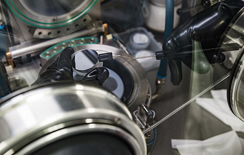
Researchers at Rochester Institute of Technology (RIT) in the US have applied a more efficient fabricating process called I-MacEtch, or inverse metal-assisted chemical etching method, to InGaP.
"What is novel about our work is that for the first time we are looking at applying I-MacEtch processing to InGaP materials. I-MacEtch is an alternative to two conventional approaches and is a technique that has been used in the field - but the materials that have been explored are fairly limited," said Parsian Mohseni, assistant professor of microsystems engineering in RIT's Kate Gleason College of Engineering. He is also director of the EINS Laboratory at the university.
"This is a very well-known material and has applications in the electronics and solar cell industries," he said. "We are not re-inventing the wheel; we are establishing new protocols for treating the existing material that is more cost effective, and a more sustainable process."
The I-MacEtch process combines the benefits of two traditional methods - wet etching and reactive ion etching, or REI. Both processes have been used to develop the electronic patterns on circuits and use silicon as a foundation for this type of patterning. Improving patterning methods by I-MacEtch could mean reducing fabrication complexity of various photonic and electronic devices.
Researchers and semiconductor fabrication scientists have been using MacEtch extensively for processing silicon. At the same time, assessments of other materials in the III-V range of individual elements that may be conducive to this same type of fabrication with similar advantages are underway. In his research, Mohseni is also looking at different alloys of those III-V materials, namely the ternary alloys such as InGaP.
The research detailed in the upcoming issue of the American Chemical Society's Applied Materials and Interfaces journal highlights how the nanofabrication methodology was applied to InGaP and how it can impact the processing of device applications and generation of high aspect ratio and nano-scale semiconductor features, said Thomas Wilhelm, a microsystems engineering doctoral student and first-author of the paper. The novel processing method can be significant in the development of ordered arrays of high aspect ratio structures such as nanowires.
For solar cells, the goal is to minimise the cost-to-power-produced ratio, and if it is possible to lower the cost of making the cell, and increasing the efficiency of it, this improves the device overall. Exploring new methods of fabricating the existing, relevant materials in a way that allows for faster, less expensive and more controlled processing by combining the benefits of wet etching and RIE has been the focus of Mohseni's work. The improved process means avoiding expensive, bulky, hazardous processing methods.
"We are using a simple benchtop set up and we end up with very similar structures; in fact, one can argue that they are higher in quality than the structures that we can generate with RIE for a fraction of the cost and with less time, less steps throughout, without the higher temperature conditions or expensive instrumentation," he said.


