
Lund University Chooses Eulitha DUV litho system
PhableR 100 DUV nano-lithography system will be used to develop nanowire devices
Eulitha, a Swiss startup company offering lithography equipment and services for the nanotechnology, photonics and optoelectronic markets has received an order for one of its unique PhableR 100 DUV photolithography systems from Lund University in Sweden.
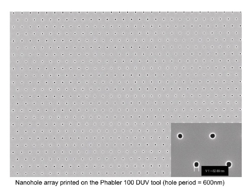
The PhableR 100 DUV exposure tool incorporates Eulitha's proprietary Displacement Talbot Lithography technology that is said to enable robust printing of very high-resolution periodic patterns at low-cost. The system ordered by the Lund University operates with a 193 nm ArF excimer laser which enables printing of features much smaller than 100 nm.
The new tool will be installed at the nano-fabrication facility, Lund Nano Lab (LNL), which is operated by NanoLund, the Centre for Nanoscience at Lund University.
LNL has more than 80 installed processing tools, including various epitaxial systems, patterning tools and characterisation equipment, serving the needs of more than 150 users from academic research groups and industry.
Maria Huffman, operations manager at the Lund Nano Lab said: "We are grateful to both the University's Faculty of Engineering (LTH) and NanoLund for granting us the funding to purchase the PhableR 100 DUV system. Also, we are very pleased that the technical leadership of Hexagem AB shared with us their data on GaN nanowires grown on substrates patterned on the Eulitha tool, which enabled us to evaluate the tool in a very efficient and effective manner.
"We believe this Displacement Talbot Lithography system will be useful to a variety of research projects and applications within the NanoLund research community. It will not only provide added capabilities currently lacking at the LNL but will also be a unique tool within Sweden. We hope that such a capability will attract various researchers, both locally and nationally."
She added, "This equipment will let us address the feature size range of 90-100 nm, which makes it very attractive to all nanowire growers within the research community, in particular those working on LED and solar cell development. One key advantage is the fact that this is a non-contact technique, perfectly suitable for sensitive substrates."
The PhableR 100 DUV system can expose periodic patterns with feature sizes well below 100nm, which rivals the performance of much more expensive state-of-the-art steppers. The patented focus-free imaging of the technology enables uniform printing on non-flat substrates often employed in photonic and optoelectronic sectors. Eulitha has previously announced the delivery of lithography systems to the University of Bath in the UK and Waterford Institute in Ireland.
Eulitha AG is a spin-off company of the Paul Scherrer Institute, Switzerland. It specializes in the development of lithographic technologies for applications in optoelectronics and photonics. In addition to photolithographic exposure machines, it produces and markets nano-patterned substrates and templates. PHABLE is a registered trade mark and the brand name of Eulitha's proprietary photolithography platform, which includes exposure tools and wafer patterning services.


