
Gallium oxide shows high electron mobility
Ga2O3 shows promise for high-frequency communication systems and energy-efficient power electronics
In new experiments reported in Applied Physics Letters, researchers have shown that the wide-bandgap semiconductor gallium oxide (Ga2O3) can be engineered into nanometer-scale structures that allow electrons to move much faster within the crystal structure. With electrons that move with such ease, Ga2O3 could be a promising material for applications such as high-frequency communication systems and energy-efficient power electronics.
"Gallium oxide has the potential to enable transistors that would surpass current technology," said Siddharth Rajan of Ohio State University, who led the research.
Because Ga2O3 has one of the largest bandgaps of the wide bandgap materials being developed as alternatives to silicon, it's especially useful for high-power and high-frequency devices. It's also unique among wide bandgap semiconductors in that it can be produced directly from its molten form, which enables large-scale manufacturing of high-quality crystals.
For use in electronic devices, the electrons in the material must be able to move easily under an electric field, a property called high electron mobility. "That's a key parameter for any device," Rajan said. Normally, to populate a semiconductor with electrons, the material is doped with other elements. The problem, however, is that the dopants also scatter electrons, limiting the electron mobility of the material.
To solve this problem, the researchers used a technique known as modulation doping. The approach was first developed in 1979 by Takashi Mimura to create a GaAs HEMT, which won the Kyoto Prize in 2017. While it is now a commonly used technique to achieve high mobility, its application to Ga2O3 is something new.
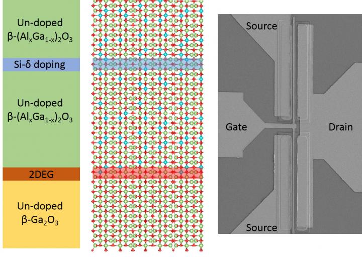
In their work, the researchers created a semiconductor heterostructure, creating an atomically perfect interface between Ga2O3 and its alloy with aluminum, aluminum gallium oxide - two semiconductors with the same crystal structure but different energy gaps. A few nanometers away from the interface, embedded inside the aluminum gallium oxide, is a sheet of electron-donating impurities only a few atoms thick. The donated electrons transfer into the Ga2O3, forming a 2-D electron gas. But because the electrons are now also separated from the dopants (hence the term modulation doping) in the aluminum gallium oxide by a few nanometers, they scatter much less and remain highly mobile.
Using this technique, the researchers reached record mobilities. The researchers were also able to observe Shubnikov-de Haas oscillations, a quantum phenomenon in which increasing the strength of an external magnetic field causes the resistance of the material to oscillate. These oscillations confirm formation of the high mobility 2-D electron gas and allow the researchers to measure critical material properties.
Rajan explained that such modulation-doped structures could lead to a new class of quantum structures and electronics that harnesses the potential of Ga2O3.
The picture above is a schematic stack and the scanning electron microscopic image of the β-(AlxGa1-x)2O3/Ga2O3 modulation-doped field effect transistor.
'Demonstration of high mobility and quantum transport in modulation-doped β-(AlxGa1-x)2O3/Ga2O3 heterostructures' by Yuewei Zhang et al; Applied Physics Letters April 24, 2018


