Loading...
News Article

HexaTech Launches 2inch AlN line

News

Breakthrough in commercial AlN substrate capability

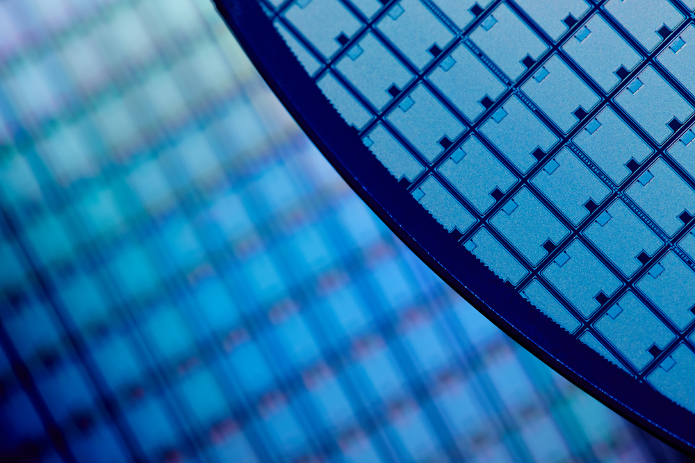
HexaTech has announced the launch of its 2inch diameter AlN substrate product line in conjunction with theInternational Conference on UV LED Technologies & Applications (ICULTA-2018) in Berlin, Germany.

"This achievement is the result of our intense, focused research and development activities, producing critical breakthroughs in AlN crystal growth performance," noted John Goehrke, HexaTech CEO. He added, "Together with strong support from our strategic partners, including Osram as announced last year, we have again raised the bar for AlN substrate technology."

Gregory Mills, VP of Business Development for HexaTech said:"This capability is the leading edge of a long-term, production-oriented product portfolio, which will enable our customers to quickly and easily transition deep-ultraviolet (UV-C) optoelectronic/electronic device development and production to an AlN substrate platform, delivering superior device performance coupled with cost-effective production scaling, process integration, and accelerated time to market."

"By challenging perceived constraints and aggressively pursuing solutions at each step of the crystal growth process, we have developed a significant shift in capability which breaks previously observed limitations. An outstanding team effort is responsible for this milestone, and sets the stage for both continued diameter expansion and increased process yields, ultimately rivaling the price:performance ratio of other mature compound semiconductor technologies, such as SiC and GaAs," stated Raoul Schlesser, HexaTech co-founder and VP of Crystal and Wafer Development.

Double heterostructure HEMTs for handsets
AlixLabs to collaborate with Linköping University
SiC MOSFETs: Understanding the benefits of plasma nitridation
Wolfspeed reports Q2 results
VueReal secures $40.5m to scale MicroSolid printing
Mitsubishi joins Horizon Europe's FLAGCHIP project
Vishay launches new high voltage SiC diodes
UK team leads diamond-FET breakthrough
GaN adoption at tipping point, says Infineon
BluGlass files tuneable GaN laser patents
QD company Quantum Science expands into new facility
Innoscience files lawsuit against Infineon
Riber revenues up 5% to €41.2m
Forvia Hella to use CoolSiC for next generation charging
Photon Design to exhibit QD simulation tool
Ortel transfers CW laser fabrication to Canada
Luminus adds red and blue multi-mode Lasers
PseudolithIC raises $6M for heterogeneous chiplet tech
Mesa sidewall design improves HV DUV LEDs
IQE revenue to exceed expectations
'Game-changing' VCSEL system targets clinical imaging
German start-up secures finance for SiC processing tech
Macom signs preliminaries for CHIPS Act funding
IQE and Quintessent partner on QD lasers for AI
EU funds perovskite tandems for fuel-free space propulsion
EU to invest €3m in GeSi quantum project
Transforming the current density of AlN Schottky barrier diodes
Turbocharging the GaN MOSFET with a HfO₂ gate
Wolfspeed launches Gen 4 SiC MOSFET technology
Report predicts high growth for UK's North East
Element Six unveils Cu-diamond composite
SemiQ launches hi-rel 1700V SiC MOSFETs
×
Search the news archive

To close this popup you can press escape or click the close icon.
Logo
x
Logo
×
Register - Step 1

You may choose to subscribe to the Compound Semiconductor Magazine, the Compound Semiconductor Newsletter, or both. You may also request additional information if required, before submitting your application.


Please subscribe me to:


You chose the industry type of "Other"

Please enter the industry that you work in: