
UK 2D materials start-up closes £2.9m seed round
Paragraf to drive first ever large-scale production of 2D based technologies
Paragraf, a recent spin out from the Centre for Gallium Nitride group of Colin Humphreys in the Department of Materials Science at the University of Cambridge, has closed a £2.9 million seed round to support the development of its first major products. The round is led by Cambridge Enterprise, the commercialisation arm of the University of Cambridge, with the participation of Parkwalk Advisors, Amadeus Capital Partners, IQ Capital Partners and angel investors.
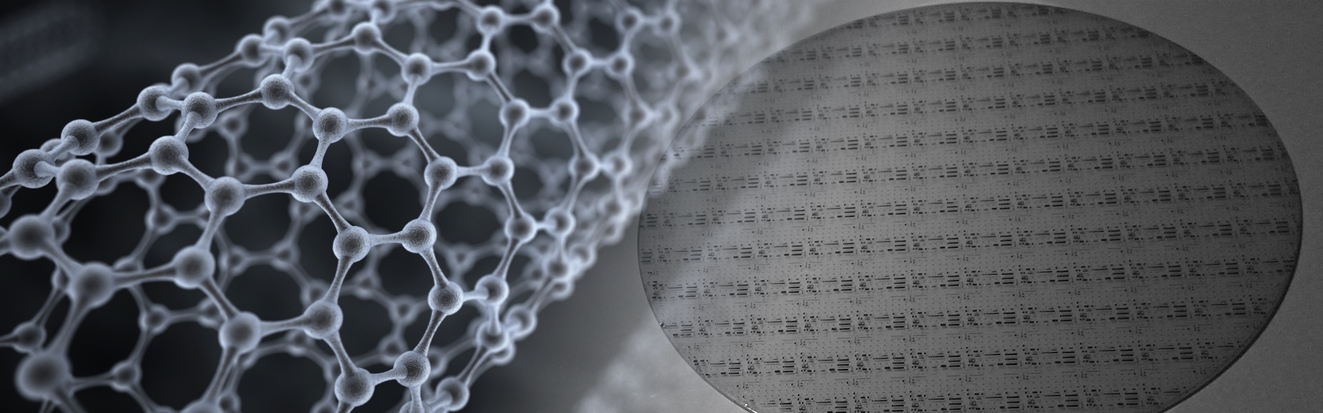
Paragraf focuses on the production of 2D materials and the development of electronic devices based on these materials. It is starting with graphene and harnessing the extremely high conductivity, superb strength, very low weight and ultimate flexibility of the material.
Simon Thomas, CEO and co-founder of Paragraf, said: "There's no doubt that the electronic, mechanical and optical properties of two-dimensional materials such as graphene have the potential to significantly increase performance in a multitude of state of the art technologies. However, until materials like graphene can be delivered in commercially viable, device compatible, functionally targeted forms, the achievements demonstrated at lab scale will not be transferred to real-world products. At Paragraf we have developed the first production technique that allows true scaling of graphene based devices."
Using a proprietary, patent protected approach Paragraf has overcome the problems of poor uniformity, reproducibility, limited size and material contamination that have stymied all current graphene manufacturing techniques. The company has already produced layers with electrical characteristics optimised for producing very sensitive detectors at commercial scale and improved efficiency contact layers for common technologies such as LEDs.
Paragraf's devices will target markets including transistors; chemical and electrical sensors; and novel energy generation devices tapping into kinetic and chemical green energy sources yet to be exploited by any other technology.
Colin Humphreys, chairman and co-founder of Paragraf, said: "Graphene has been called the new wonder material, because of its potential to transform a range of industries such as electronics, energy and healthcare. However, so far, its applications have been limited because good quality graphene is only available in small flakes. Our underlying research has the capability to transform production by providing good quality, large-area graphene on a commercial scale."
Hermann Hauser, co-founder of Amadeus Capital Partners, remarked: "Graphene has demonstrated some remarkable achievements in the lab, showing great promise for many future electronic technologies. However, without a pathway to commercial viability, scaling from proof of concept to end user accessible products remains beyond the horizon. Paragraf's novel approach to two-dimensional materials fabrication brings the possibility of mass market graphene based devices a step closer to reality."


