
Scientists make semiconductor nanoribbons from speeding droplets
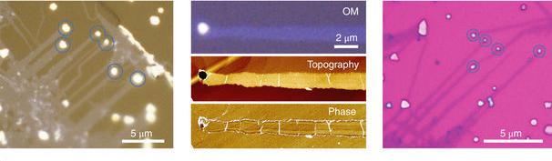
From left to right: 1) optical images of MoS2 ribbons grown on a NaCl crystal, 2) optical microscopy and corresponding AFM topography and phase images of a ribbon, and 3) optical image of the ribbons transferred onto a SiO2/Si substrate.
An international team of researchers, affiliated with the Ulsan National Institute of Science and Technology in South Korea (UNIST) has discovered a novel method for the synthesis of 2D semiconductors. The unique growth mechanism yielded nanoscopic semiconductor ribbons that are only a few atoms thick.
This breakthrough has been jointly conducted by Feng Ding and Wen Zhao from the Centre for Multidimensional Carbon Materials (CMCM), within the Institute for Basic Science (IBS) at UNIST, in collaboration with the National University of Singapore (NUS), the National Institute for Materials Science (NIMS), the National Institute of Advanced Industrial Science and Technology (AIST), and Shenzhen University.
In the study, the research team successfully fabricated MoS2 nanoribbons via vapour-liquid-solid (VLS) growth mechanism, a type of chemical vapour deposition (CVD) process.
In the study, Zhao performed density functional theory based molecular dynamic (DFT-MD) simulations of the MoS2 precipitation process.
The proposed mechanism of VLS growth differs from commonly known CVD technique, as it involves the precursors introduced in the vapour phase form a liquid droplet intermediate before condensing into a solid product.
The team noted that the morphology of the growth product was, however, unlike what is normally expected from a VLS growth, which typically yields cylindrical or tubular structures rather than ribbons.
Their observation suggests that the liquid droplet migrates on the substrate surface in a rather ordered manner, leaving behind a track of ultrathin crystal.
"Because the liquid droplet migrates on the substrate surface in a rather ordered manner, the morphology of the growth product yielded cylindrical or tubular structures rather than ribbons," says Zhao.
This time, however, the horizontal growth of predominantly monolayer MoS2 ribbons was obtained via VLS growth, a unique growth mechanism that has not been reported until now.
Their observation revealed that the VLS growth of monolayer MoS2 is triggered by the reaction between MoO3 and NaCl, which results in the formation of molten Na-Mo-O droplets. These droplets mediate the growth of MoS2 ribbons in the 'crawling mode' when saturated with sulphur. The locally well-defined orientations of the ribbons reveal the regular horizontal motion of the droplets during growth.
In order to gain insight into the liquid-solid transformation, Ding's team performed density functional theory based molecular dynamic (DFT-MD) simulations of the precipitation process. The simulation showed the attachment of molybdenum and sulphur to the previously established MoS2.
"It is worth noting that MoS2 is not oxidised despite the presence of large numbers of oxygen atoms," says the research team. "We also observe the nucleation of MoS2 clusters in regions that are rich in Mo and S atoms, further supporting the feasibility of liquid-mediated nucleation and growth of MoS2."
"This study has prompted questions about surface and interface growth of nanomaterials," says Ding. "By identifying a suitable liquid-phase intermediate compound, we believe that it will be possible to realise the direct 1D growth of a range of van der Waals layered materials."
The team anticipates that many other materials can be grown using a similar approach. Their short-term goal is to understand the growth mechanism better and to control the morphology of the ribbons.
"Our work identified many interesting questions about surface and interface growth of nanomaterials," says Goki Eda at the National University of Singapore (NUS), the corresponding author of this study. "We predict that the ability to directly grow complex structures will greatly facilitate the realisation of high performance nanoelectronic circuits."
The team noted that their results provide insight into the distinct VLS growth mode of 2D MoS2 and demonstrate the potential of their implementation in nanoelectronic devices. The findings of this study have been published in Nature Materials on April 23, 2018.
'Vapor-Liquid-Solid Growth of Monolayer MoS2 Nanoribbons' by Shisheng Li, et al; Nat. Mater. (2018).


