
Siltectra adds GaAs to Cold Split list
At SEMICON West, Siltectra, a Germany-based wafering technology firm, has revealed new enabling and cost-of-ownership (CoO) advantages for its Cold Split technology. Collectively, the benefits aim to further enable manufacturers of power semiconductors.
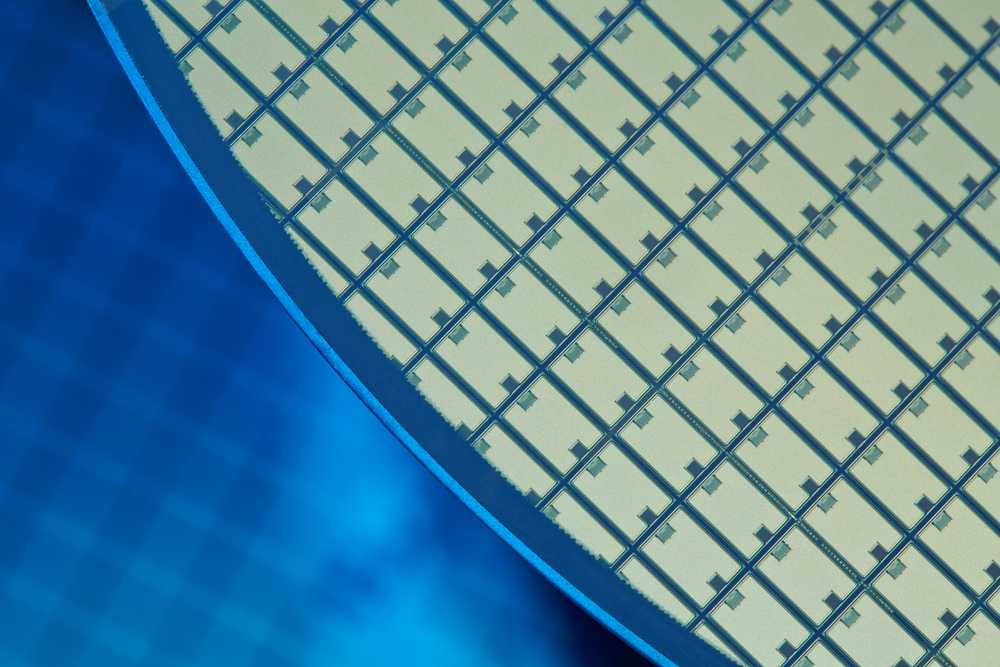
In the latest demonstration of Cold Split's capabilities, Siltectra said that when applied to GaAs, Cold Split achieved the same breakthrough thinness and near-zero material loss as previously shown for SiC, GaN, sapphire and silicon.
The data comes from a recent study funded by the State Government of Saxony. The study aimed to establish if Cold Split could achieve full crack propagation across the laser plane when applied to GaAs. Participants included a leading materials supplier and a renowned laser institute, as well as Siltectra. The results validated Cold Split as a high-performance thinning solution for GaAs and demonstrated that the technique can successfully thin a range of diverse materials with complex properties.
The data builds on feedback from Cold Split customers who found that the novel thinning technique is demonstrating strong CoO advantages when compared to traditional grinding. Not only can Cold Split thin wafers to 50 microns and below in minutes, it produces virtually no material loss. Grinding is a slower process and can incur material waste of up to 90 percent. And now, thanks to an adaptation known as 'twinning', Cold Split users can reclaim substrate material generated (and previously wasted) during backside grinding and create a fully optimizable bonus wafer. Siltectra believes that these benefits can cut consumables costs by 50 percent and reduce overall wafering costs by as much as 30 percent.
"Significantly lower consumables costs are a key driver of Cold Split's compelling CoO, especially for SiC-based devices," said Siltectra's CTO, Jan Richter. "While the industry is starting to adopt SiC for power semiconductors, it is an extraordinarily hard substance. Every single micron must be ground and polished, micron-by-micron. Grinding involves expensive diamond-based consumables, and when coupled with the technique's inherent material waste, costs can be high. In contrast, Cold Split produces almost no waste which vastly reduces consumables costs. And because the technique can save virtually every micron of SiC and turn surplus material into a bonus wafer, CoO is further boosted."
Siltectra's CEO, Harald Binder remarked that the new data may also have exciting performance implications for end-user devices. "Take low-voltage SiC-based SCHOOTKY diodes, for example," he said. "With these diodes, low resistance is essential to reducing electrical losses in end-user applications. The thickness of the final device influences resistance. The thinner the device, the lower the resistance. Reducing thickness, therefore, can decrease resistance and reduce electrical losses. This means that in addition to low-cost/high-speed wafer thinning, Cold Split can potentially also improve the electrical performance of low-voltage devices."
Binder concluded: "Much of our new data is occurring in real time as the industry shifts fast to new materials. That said, the innovation has been happening at Siltectra for many years and is protected by 70 patent families covering technology, manufacturing equipment, materials and expertise. It is gratifying to see our discoveries exceeding even their original promise as we collaborate with manufacturers to help them achieve aggressive roadmap goals."


