
UCLA team shows merits of BAs for heat management
Working to address "˜hotspots' in computer chips that degrade their performance, UCLA engineers have developed a new semiconductor material, defect-free boron arsenide (BAs), that they say is more effective at drawing and dissipating waste heat than any other known semiconductor or metal materials.
The results of the study, led by Yongjie Hu, UCLA assistant professor of mechanical and aerospace engineering, were published in the journal Science.
Managing heat in electronics has become one of the biggest challenges in optimising performance. There are two main reasons. First, as transistors shrink in size (under Moore's Law, the number of transistors on a chip doubles about every two years), more heat is generated within the same footprint. The high heat slows down processor speeds, in particular at "˜hotspots' on chips where heat concentrates and temperatures soar. Second, a lot of energy is used to keep those processors cool. If CPUs did not get as hot in the first place, then they could work faster and much less energy would be needed to keep them cool.
The UCLA study was the culmination of several years of research by Hu and his students that included designing and making the materials, predictive modelling, and precision measurements of temperatures.
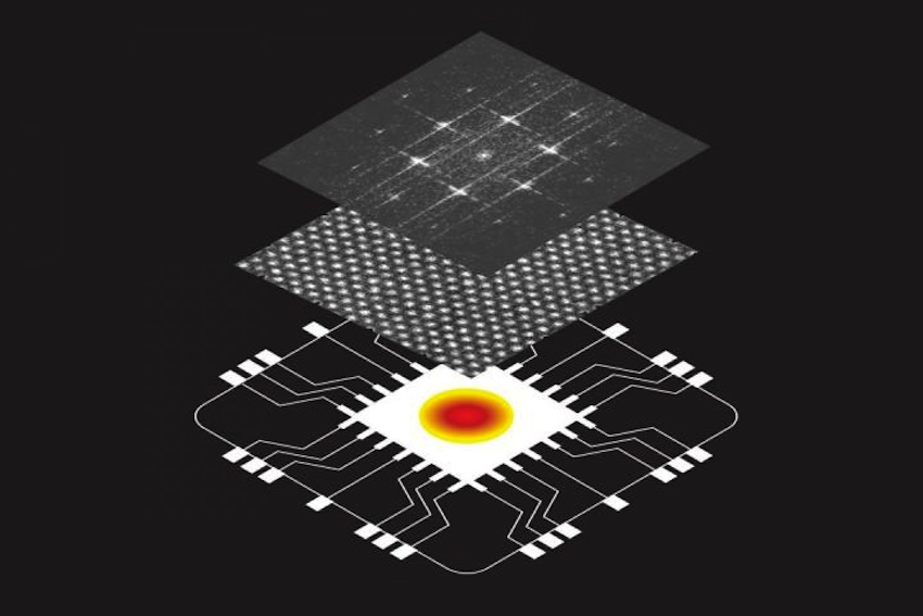
UCLA's defect-free BAs has a record-high thermal conductivity, more than three-times faster at conducting heat than currently used materials, such as SiC and copper, so that heat that would otherwise concentrate in hotspots is quickly flushed away. The Illustration above shows a schematic of a computer chip with a hotspot (bottom); an electron microscope image of defect-free boron arsenide (middle); and an image showing electron diffraction patterns in BAs.
"This material could help greatly improve performance and reduce energy demand in all kinds of electronics, from small devices to the most advanced computer data center equipment," Hu said. "It has excellent potential to be integrated into current manufacturing processes because of its semiconductor properties and the demonstrated capability to scale-up this technology. It could replace current state-of-the-art semiconductor materials for computers and revolutionise the electronics industry."
In addition to the impact for electronic and photonics devices, the study also revealed new fundamental insights into the physics of how heat flows through a material.
"This success exemplifies the power of combining experiments and theory in new materials discovery, and I believe this approach will continue to push the scientific frontiers in many areas, including energy, electronics, and photonics applications," Hu said.
The research was funded by the National Science Foundation, the Air Force Office of Scientific Research, the American Chemical Society's Petroleum Research Fund, UCLA's Sustainable LA Grand Challenge, and the Anthony and Jeanne Pritzker Family Foundation.
'Experimental observation of high thermal conductivity in boron arsenide' by Joon Sang Kang et al; Science 05 Jul 2018


