
EPFL develops room temperature exciton-based transistor
Researchers at the à‰cole polytechnique fédérale de Lausanne (EPFL) have created a transistor using excitons instead of electrons. The transistor, which is based on the 2D compound semiconductors WSe2 and MoS2, functions effectively at room temperature, a hitherto insurmountable obstacle.
They think their study, which was published in Nature, has numerous implications in the field of excitonics, one of the most promising new areas of study alongside photonics and spintronics.
"Our research showed that, by manipulating excitons, we had come upon a whole new approach to electronics," says Andras Kis, who heads EPFL's Laboratory of Nanoscale Electronics and Structures (LANES). "We are witnessing the emergence of a totally new field of study, the full scope of which we don't yet know."
This breakthrough sets the stage for optoelectronic devices that consume less energy and are both smaller and faster than current devices. In addition, it will be possible to integrate optical transmission and electronic data-processing systems into the same device, which will reduce the number of operations needed and make the systems more efficient.
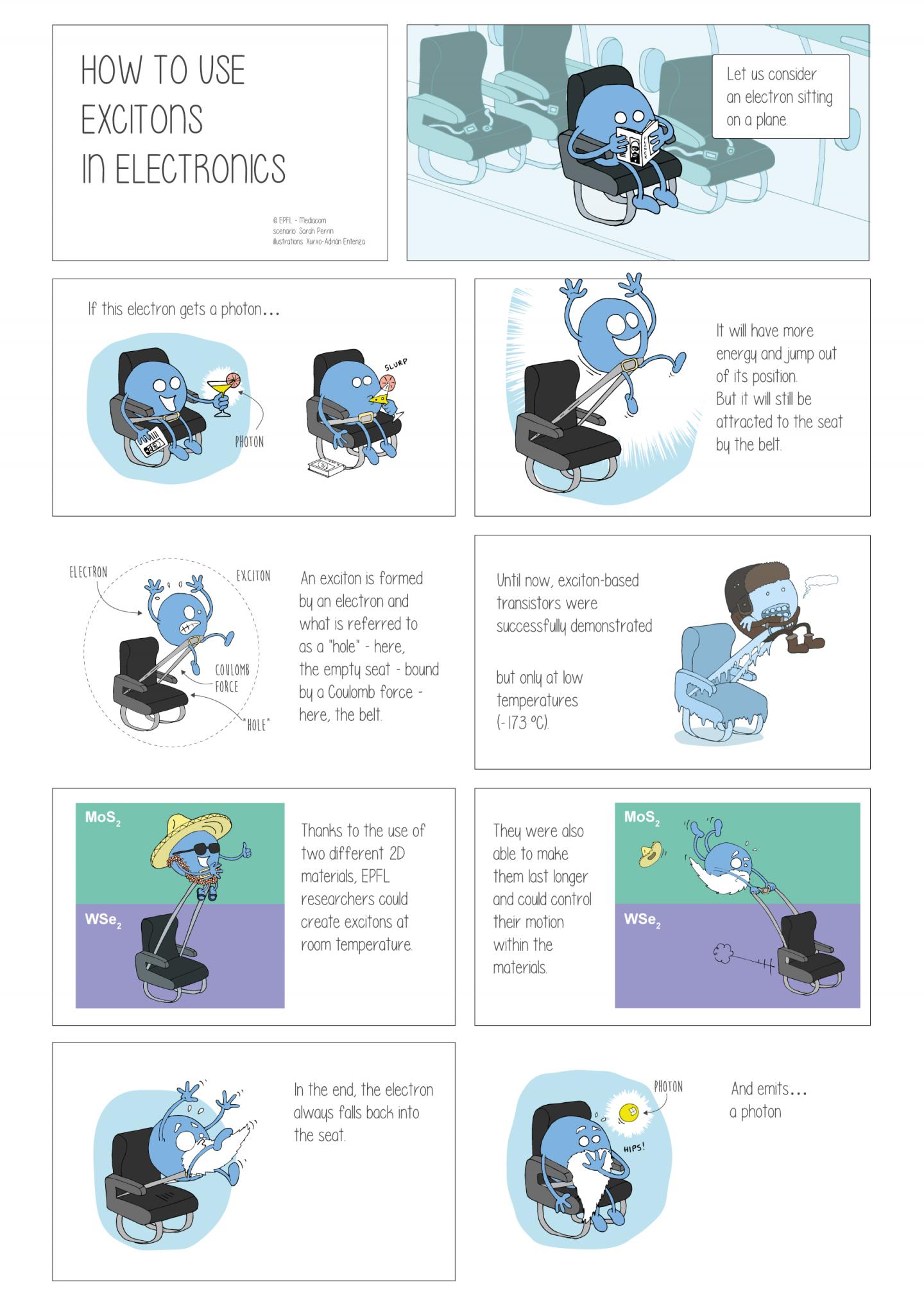
Higher energy level
Excitons are quasiparticles, a term used to describe the interaction between the particles that make up a given substance rather than the substance itself. Excitons consist of an electron and an electron hole. The two are bound together when the electron absorbs a photon and achieves a higher level of energy; the 'excited' electron leaves behind a hole in the previous level of energy, which, in band theory, is called a valence band. This hole, also a quasiparticle, is an indication of the missing electron in this band.
Since the electron is negatively charged and the hole is positively charged, the two particles remain bound by an electrostatic force. This bond between the electron and the hole is called Coulomb attraction. And it is in this state of tension and balance that they form an exciton. When the electron finally falls back into the hole, it emits a photon. And with that, the exciton ceases to exist. Put more simply, a photon goes in at one end of the circuit and comes out the other; while inside, it gives rise to an exciton that acts like a particle.
Double success
It is only recently that researchers have begun looking at the properties of excitons in the context of electronic circuits. The energy in excitons had always been considered too fragile and the excitons' life span too short to be of any real interest in this domain. In addition, excitons could only be produced and controlled in circuits at extremely low temperatures (around -173degC).
The breakthrough came when the EPFL researchers discovered how to control the life span of the excitons and how to move them around. They did this by using two 2D materials: WSe2 and MoS2. "The excitons in these materials exhibit a particularly strong electrostatic bond and, even more importantly, they are not quickly destroyed at room temperature," explains Kis.
The researchers were also able to significantly lengthen the excitons' life span by using the fact that the electrons always found their way to the MoS2 while the holes always ended up in the WSe2. And, working with two Japanese researchers, they kept the excitons going even longer by protecting the semiconductor layers with boron nitride (BN).
"We created a special type of exciton, where the two sides are farther apart than in the conventional particle," says the researcher. "This delays the process in which the electron returns to the hole and light is produced. It's at this point, when the excitons remain in dipole form for slightly longer, that they can be controlled and moved around using an electric field."
'Room-temperature electrical control of exciton flux in a van der Waals heterostructure' by Dmitrii Unuchek et al; Nature 25 July 2018


