Affordable way to print bendy ZnO nanowires

In a paper just published in the journal Microsystems and Nanoengineering, engineers from the University of Glasgow have described how they have for the first time been able to affordably "˜print' high-mobility semiconductor nanowires onto flexible surfaces to develop high-performance ultra-thin electronic layers.
Those surfaces, which can be bent, flexed and twisted, could lay the foundations for a wide range of applications including video screens, improved health monitoring devices, implantable devices and synthetic skin for prosthetics.
The paper is the latest development from the University of Glasgow's Bendable Electronics and Sensing Technologies (BEST) research group, led by Ravinder Dahiya.
In their paper, the research team outline how they manufactured semiconductor nanowires from both silicon and ZnO and printed them on flexible substrates to develop electronic devices and circuits. In the process, they discovered that they could produce uniform silicon nanowires which aligned in the same direction, as opposed to the more random, tree-branch-like arrangement produced by a similar process for ZnO.
Since electronic devices run faster when electrons can run in straight lines as opposed to having to negotiate twists and turns, the silicon nanowires were best suited to use in their flexible surfaces.
From there, the team engaged in a series of experiments to print the wires into flexible surfaces with a printing device they developed and built in their lab. After a series of experiments, they were able to find the optimal combination of pressure and velocity to effectively print the nanowires time after time.
Dahiya said: "This paper marks a really important milestone on the road to a new generation of flexible and printed electronics. In order for future electronic devices to integrate flexibility into their design, industry needs to have access to energy-efficient, high-performance electronics which can be produced affordably and over large surface areas.
"With this development, we've gone a long way to hitting all of those marks. We've created a contact-printing system which allows us to reliably create flexible electronics with a high degree of reproducibility, which is a really exciting step towards creating all kinds of bendable, flexable, twistable new devices.
"We've just secured further funding which we'll use to scale up the process further, making it more readily applicable to industrial purposes, and we're looking forward to building on what we've managed to achieve already."
Pictured above:
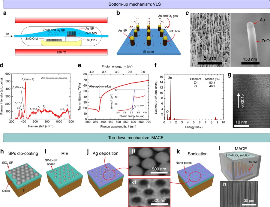
a"“g Bottom-up ZnO NWs grown by CVT. a 2D schematic illustration of CVT process. b 3D schematic illustration detailing VLS growth mechanism of ZnO NWs using Au NPs as catalyst. c SEM images of ZnO NWs vertically aligned on Si(111) substrate. Characterisation of ZnO NWs by d Raman spectroscopy, e transmission spectrophotometry, f EDX, and g TEM. Inset of (e) shows Tauc's plot for Eg analysis.
h"“l Top-down Si NWs grown by MACE. h"“k 3D schematic illustration of MACE process, comprising (h) large-area dip-coating of SiO2 SPs on Si(100) substrate, i SPs size reduction by RIE, j Ag deposition by thermal evaporation (j1: SEM image), k SP removal by sonication (k1: SEM image), and l MACE synthesis (l1: SEM image)


