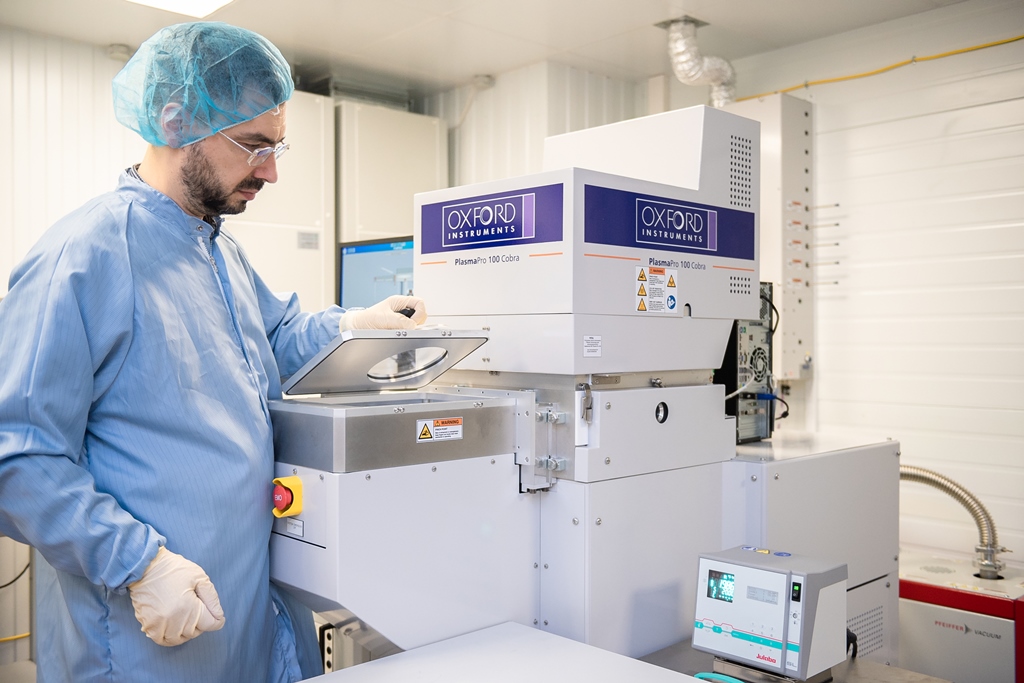
Siberian team working on next generation semiconductors

Scientists at Tomsk State University in Siberia and their industrial partner Mikran, a Siberian electronics firm, are creating the technology of industrial production of thin-film semiconductor heterostructures for civil, defence, and space products. In particular, they are developing HEMTs for cellular, satellite, and radio communication at high frequencies.
"The problem of increasing the specific power of transistors and thereby their long-range response will be solved with the help of a new chemical composition of semiconductor materials used for the production of heterostructures," says Valentin Brudnyi, professor at the Department of the Physics of Semiconductors, the scientific director of the project, and director of the Research Educational Centre Nanoelectronics. "For the production of modern HEMT, multilayer thin-film heterostructures are used. Their functional characteristics can be improved by InAlGa nitride compounds in combinations that were not previously used industrially."
While HEMTs made from GaAs, InAs, and GaSb provide high operating frequencies, they have small output powers due to the peculiarities of their electronic properties. But using semiconductor nitrides for the production of HEMT transistors and, in particular InAlN/GaN heterostructures, will increase their specific power, thermal stability, and resistance to external high-energy impacts, says Brudnyi.
During the manufacture of HEMT, the volatile metal-organic compounds will be applied layer-by-layer to a SiC subsurface. The total thickness of all layers will be several micrometers (1 μm = 10â»â¶ meters).
Work on creating HEMT based on InAlN/GaN heterostructures has been underway in a number of firms around the world, but industrial production is currently lacking. Upon completion of the project, TSU will prepare the technological documentation for transfer to Mikran, which will commence the industrial production of such NEMT transistors.


