
Agnitron Develops Gallium Oxide MOCVD Capability
Agnitron Technology, a US compound semiconductor technology company, has developed a new MOCVD growth capability which delivers an order of magnitude improvement to background concentration levels for beta-phase Gallium Oxide (ββ-Ga2O3) films.
The development has resulted in achievement of a new record, regardless of deposition technique, for room and low temperature bulk film mobilities in ββ-Ga2O3. This advance is key to realising potential of the material system for operating at high voltages "“ an application with broad interest for the 4.9eV bandgap semiconductor. Calculations indicate this new capability will support fabrication of field effect transistor devices capable of operating beyond 10kV. The new growth capability was presented at the 2018 US Workshop on Gallium Oxide at Ohio State University, Columbus, Ohio, August 15-16.
ββ-Ga2O3 and other wide bandgap semiconductors exhibit material properties which will allow power electronic switches to improve performance in a range of categories meaning lower on-resistance and switching losses, higher operating temperatures and higher frequency operation. If realised, these improvements will allow many types of voltage converter systems to reduce size, weight, and complexity while improving energy efficiency. Over time this could translate to improved performance and tremendous energy savings on a large scale for electric drive vehicles, transportation infrastructure and distributed/renewable energy systems among others.
The Agnitron team, led by president and program PI Andrei Osinsky, recently performed a series of experiments to better understand just how good MOCVD grown ββ-Ga2O3 films can be. "It was clear that reducing background concentration is critical to the future commercial viability of ββ-Ga2O3. Thus, we focused on optimising a number of key reactor and process parameters and managed to grow films with surprisingly low levels," said Osinsky. "There is much more work to do but already a number of recent runs have produced films near 10µm thick and shown the improved process can reproducibly offer background concentration levels in the ~5E15 cm-3 range as measured by CV and Hall measurement techniques." Osinsky added that the lowest concentration measured to date was by CV with an Nd-Na value of 3E15 cm-3.
These low background concentrations have led to observing electron mobilities in the films at room and low temperature of 174 cm2/(V·s) and 2800 cm2/(V·s), respectively "“ new records for the material based on published literature. The films also have been produced with surface roughness levels <0.2nm RMS which is an important property for both lateral and vertical conducting devices.
James Speck of UCSB has collaborated with Agnitron over the course of the last two years on multiple ββ-Ga2O3 projects and his group performed measurements on the reported films. Speck commented that, "This new capability by Agnitron sets yet another record for ββ-Ga2O3 mobilities by MOCVD or any technique. It is a critical development for pushing voltage performance of power transistors higher and opens the door for a number of device types; I'm excited to see what device performance advances will follow."
A number of important device properties dictate the ultimate voltage performance of a field effect transistor. These include but are not limited to the film material properties and the dimensions and background impurity concentration of the drift layer/region. The background impurity concentration also directly influences the electron mobility of the films for all device topologies "“ generally, films require fewer impurities to achieve higher electron mobility. Since ββ-Ga2O3 exhibits a breakdown field well beyond that of silicon, SiC and GaN it means that ββ-Ga2O3 based devices can potentially be thinner or smaller while operating at the same voltages as these other materials or go to levels not otherwise possible.
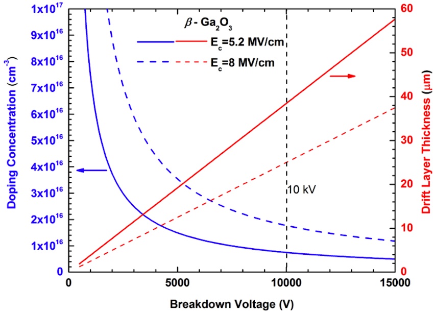
Calculations indicate a background concentration in the range now available from Agnitron's MOCVD process (~5E15 cm-3 range) will support device operation beyond 10kV (as shown in Figure 1 above), which is a new voltage performance class for field effect transistor devices.The graph above shows doping concentration (blue traces) and Drift Layer thickness (red traces) versus breakdown voltage for ββ-Ga2O3. The solid lines are for ββ-Ga2O3 layer with critical breakdown field of 5.2 MV/cm, which was experimentally demonstrated by Cornell University. The dashed lines are for ββ-Ga2O3 layer with the theoretical critical breakdown field of 8.0 MV/cm. The vertical dashed line shows the doping concentration and the drift layer thickness needed to realise power devices that operate at a voltage of 10kV. Calculations and plot courtesy of Huili (Grace) Xing, Cornell University.
A summary article of Agnitron's ββ-Ga2O3 work was recently featured in the June issue of Compound Semiconductor (Volume 24, Issue 4) and highlights several other important MOCVD growth capabilities such as high growth rates, alloying and doping. Agnitron's ongoing ββ-Ga2O3 development work is in part supported by ONR contract number N6833518C0192, under the direction of Lynn Peterson and AFOSR contract number FA9550-17-P-0029, under the direction of Ali Sayir.
Agnitron's Agilis Series MOCVD equipment offers configurations which support material growth capabilities for III-N, As/P, oxide, 2-D/TMD and many other related materials. The Agilis ββ-Ga2O3 configuration with single or multi-wafer loading capacity reactor options is now available for the general market. Agnitron also performs contract III-N and oxide R&D services at its MOCVD growth laboratory in Eden Prairie, MN.


