
MicroLEDs: the path to cost reduction
MicroLEDs technologies are improving rapidly but the challenge now is cost reduction. What is the feasibility of each solution? Can microLED TV or smartphone display manufacturing costs be compatible with these applications? Which cost reduction paths are the most realistic?

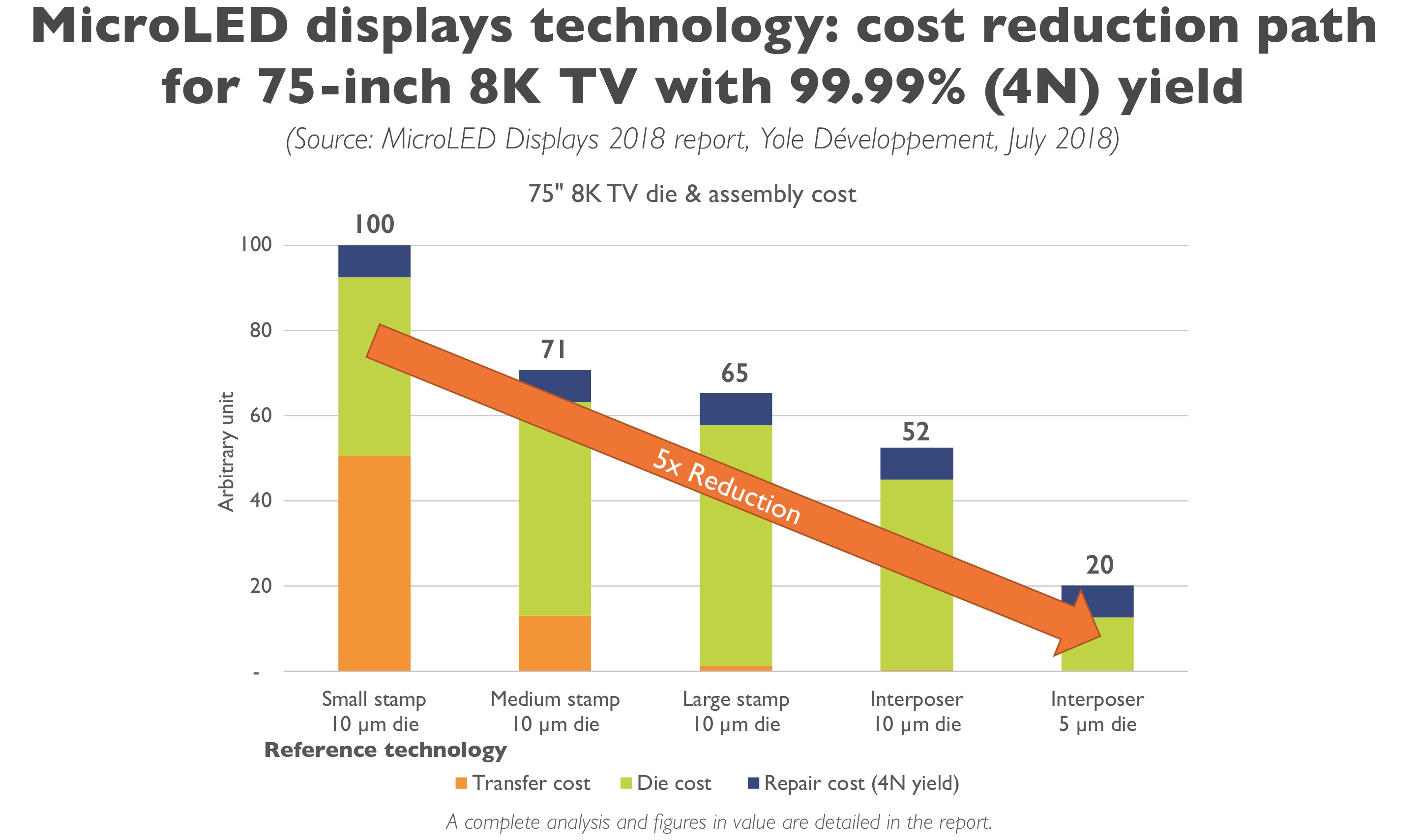
In its latest microLEDs report 'MicroLED Displays 2018', the market research and strategy consulting company Yole Développement (Yole) looks at costs and highlights the critical technology blocks and remaining challenges. "Technology advancements pave the way for various cost reduction paths toward volume manufacturing", comments Eric Virey, senior market and technology analyst at Yole. "But none are straightforward"¦"
Dozens of technologies are being developed for microLED assembly and pixel structures. The cost and complexity range can be staggering. However, there are some fundamentals that anchor all those processes. Alignment dominates assembly cycle times, die size can't get infinitely small, epitaxy cost has already been through a more than 20 years on the cost reduction curve. Cost analysis therefore allows companies to narrow the process parameters down to economically realistic windows and identify efficient cost reduction strategies.
"MicroLED companies must understand the cost targets for each application and work backward, making process choices and developing each step so it fits the cost envelope," says Virey. "Processes that can't deliver the right economics will disappear. If none can deliver the right economics, the opportunity will never materialise. MicroLED is entering the valley of death between technology development and industrialisation and commercialisation."
As the technology improves, there are credible cost reduction paths for microLED to compete in the high-end segment of various applications such as TV, augmented and virtual reality (AR/VR) and wearables. With the right approaches, assembly cost could become a minor contributor. For smartphones, however, approaching OLED cost implies pushing microLEDs toward what is likely to be the limits of the technology in term of die size.
To succeed, microLEDs will have to count on some level of price elasticity. It must deliver performance and features that no other display technology can offer and that are perceived by the consumer as highly differentiating. Microdisplays for AR and head-up displays (HUD) will be the first commercial applications, followed by smartwatches. TVs and smartphones could follow three to five years from now.


