
SemiGen upgrades manufacturing Capability
SemiGen has announced that after moving into its new state-of-the art facility, increasing assembly, foundry and screening capabilities, it has made an additional capital investment of over a half million dollars in new manufacturing and fabrication equipment to support customer demand.
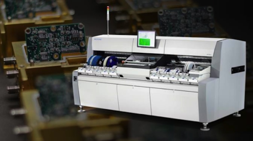
The new equipment consists of improvements across the entire service platform which include: a new Mycronic MY300 pick and place system; two new Westbond Wire bonders, a new Centrotherm eutectic vacuum chamber, new HTOL / HTRB ovens, as well as a new Disco DAD3220 dicing saw. In addition, the compn made several upgrades in the RF test department which includes new pieces of test and metrology tools.
"I'm excited to be in a position to continue to invest in and grow this important business to the RF/microwave industry," said Tim Filteau, president of SemiGen. "Our CEO, Jim Morgan, has said we must do everything we can to help our customers augment their design, assembly, and hi-rel testing and up screening capabilities, and it feels great to see this new equipment getting up and running to do just that."
SemiGen is a US-based outsource to oems in the RF/microwave, military, space, homeland security, optical, medical device, and commercial wireless markets. Its services and products are designed to fill voids in the manufacturing supply chain and production floor. SemiGen's design and manufacturing centre includes wire bonding to Si, GaAs, and GaN chips, RF/microwave and PCB assembly, mixed signal digital and analogue assembly, module repair, and high frequency testing and up- screening services.
In recent years, SemiGen has invested in coupling its services with in-stock product solutions by carrying the diodes, active and passive semiconductor devices, and bonding supplies needed for successful production of several types of solid-state, multi-function assemblies (MFAs) and components. The team helps with designs, builds prototypes, and handles volume production runs within its new 37,000 square foot facility in Manchester, NH.
The facility also includes a class 10,000 clean room. Manual to fully automatic assembly solutions are now available.RF/microwave assembly, PCB, box build, module repair and test services coupled with the semiconductor devices and manufacturing supplies needed for successful manufacturing of RF/Microwave hybrids and components. The team helps with designs, builds prototypes, and handles volume production runs for the RF/microwave, military, space, homeland security, optical, medical device, and commercial wireless markets. Its 37,000 square foot facility includes a class 10,000 clean room and offers manual to full automatic assembly solutions.
With the recent upgrades in place, SemiGen also offers wafer processing of silicon wafers, as well as processing ceramic substrates. Processing services provided include any combination of photolithography, wet etch, dry etch, metallisation, grinding, polishing, as well as in-process metrology.
The recent investments in RF test and environmental test capabilities has also enabled the company to offer high-reliability screening of amplifiers, FETs, MMICs, transistors, diodes, and other RF and microwave components operating up to mmwave frequencies.
Tests can be performed and delivered with full documentation in adherence with MIL-PRF-19500, MIL-PRF-38534, and MIL-PRF-38535 requirements. Element evaluation and screening options from Class H, Class K, TX, TXV, S-level, as well as custom SCD driven requirements are available.


