Loading...
News Article

BAE and US Air Force Lab sign GaN agreement

News
BAE will work with AFRL to establish a 140-nanometer GaN MMIC process ready for production in 2020

BAE Systems has signed a cooperative agreement with the Air Force Research Laboratory (AFRL) for Phase 1 of a technical effort to transition GaN semiconductor technology developed by the US Air Force to its Advanced Microwave Products (AMP) Center.

As part of the effort, BAE will transfer and further enhance the technology, and scale it to 6-inch wafers to slash per-chip costs and improve the accessibility of this defence-critical technology.

Under the agreement, BAE will work with AFRL to establish a 140-nanometer GaN MMIC process that will be qualified for production by 2020, with products available to Department of Defense (DoD) suppliers through an open foundry service.

"Millimeter-wave GaN technologies today are produced in research and development laboratories in low volumes at high associated costs or in captive foundries that are not broadly accessible to defense suppliers," said Scott Sweetland, Advanced Microwave Products director at BAE Systems. "This effort will leverage AFRL's high-performance technology and BAE Systems' 6-inch manufacturing capability to advance the state of the art in GaN MMIC performance, reliability, and affordability while providing broader access to this critical technology."

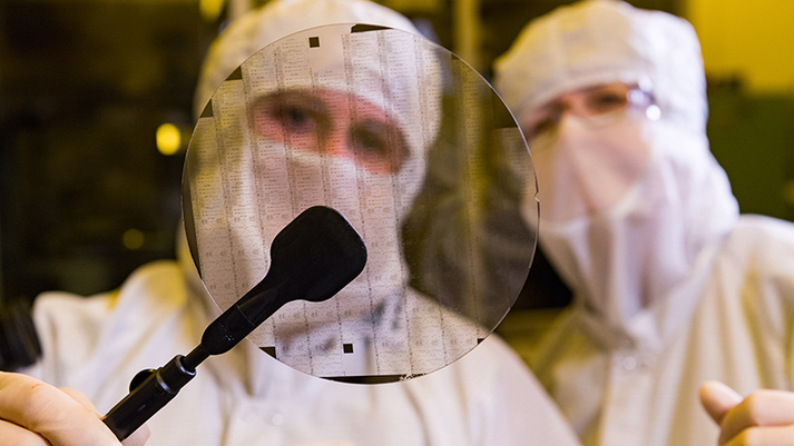
The work on this project will primarily take place in BAE's 70,000-square-foot Microelectronics Centre (MEC) in Nashua, New Hampshire, where we research, develop, and produce compound semiconductor materials, devices, circuits, and modules for a wide range of microwave and millimeter-wave applications. The MEC has been an accredited DoD Category 1A Trusted Supplier since 2008, and fabricates integrated circuits in production quantities for critical DoD programs.

As part of the project, the AMP Center team will work closely with the company's FAST LabsT research organization and MMIC design experts from ENGIN-IC.

Double heterostructure HEMTs for handsets
AlixLabs to collaborate with Linköping University
SiC MOSFETs: Understanding the benefits of plasma nitridation
Wolfspeed reports Q2 results
VueReal secures $40.5m to scale MicroSolid printing
Mitsubishi joins Horizon Europe's FLAGCHIP project
Vishay launches new high voltage SiC diodes
UK team leads diamond-FET breakthrough
GaN adoption at tipping point, says Infineon
BluGlass files tuneable GaN laser patents
QD company Quantum Science expands into new facility
Innoscience files lawsuit against Infineon
Riber revenues up 5% to €41.2m
Forvia Hella to use CoolSiC for next generation charging
Photon Design to exhibit QD simulation tool
Ortel transfers CW laser fabrication to Canada
Luminus adds red and blue multi-mode Lasers
PseudolithIC raises $6M for heterogeneous chiplet tech
Mesa sidewall design improves HV DUV LEDs
IQE revenue to exceed expectations
'Game-changing' VCSEL system targets clinical imaging
German start-up secures finance for SiC processing tech
Macom signs preliminaries for CHIPS Act funding
IQE and Quintessent partner on QD lasers for AI
EU funds perovskite tandems for fuel-free space propulsion
EU to invest €3m in GeSi quantum project
Transforming the current density of AlN Schottky barrier diodes
Turbocharging the GaN MOSFET with a HfO₂ gate
Wolfspeed launches Gen 4 SiC MOSFET technology
Report predicts high growth for UK's North East
Element Six unveils Cu-diamond composite
SemiQ launches hi-rel 1700V SiC MOSFETs
×
Search the news archive

To close this popup you can press escape or click the close icon.
Logo
x
Logo
×
Register - Step 1

You may choose to subscribe to the Compound Semiconductor Magazine, the Compound Semiconductor Newsletter, or both. You may also request additional information if required, before submitting your application.


Please subscribe me to:


You chose the industry type of "Other"

Please enter the industry that you work in: