
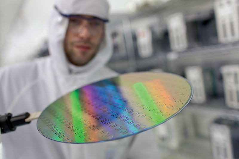
Laying foundations for vertical transistor manufacture
Semiconductor Physics made great strides in the twentieth century. Studies of this form of material in the early 1900s led to an understanding of its basic properties, along with techniques on how to dope it. Further progress came in 1947, when a team at Bell Labs produced the first point contact transistor, and three key milestones followed in the 1950s: the first single crystal germanium in 1952; the first single crystal silicon in 1954; and then, in 1958, the first IC, thanks to efforts at Texas Instruments.
Rapid improvements in the IC followed, spawning the creation of the silicon industry. And in 1965, Gordon Moore quantified the rapid rate of progress: according to his prediction, now known as "˜Moore's Law', the transistor density on a chip would double every 18 months. This is accomplished by scaling the dimensions of the transistor, a move that must go hand-in-hand with improvements in the performance of the device. To help engineers adhere to this, in 1974 Robert Dennard and co-workers at IBM proposed a set of rules for transistor scaling.
Keeping pace with Moore's Law, while following the guidelines of Dennard, has led to a period of extensive scaling. Performance and power specifications have been fulfilled at every new node, allowing the cost per chip to plummet. The enabler behind all this progress has been the innovation in process integration (see Figure 1).
Up until about a decade ago, advances in lithography held the key to performance improvement. But in recent times, there have been issues that can't be addressed by just lithography, so other innovations have had to drive progress.
One of the big changes to the transistor has been the replacement of the SiO2 dielectric with HfO2. Driving this change is that the shrinking of the MOSFET leads to an increase in gate leakage current, due to direct tunnelling, so to combat this, Intel introduced HfO2/metal gates in its 45 nm technologies that were introduced in 2007.
Another recent challenge has been maintaining a reduction in power density. For many years, decreasing the applied voltage did the trick. However, that is no longer an option for silicon, with reductions in voltage compromising on-state performance. To address this, chipmakers introduced multi-core architectures in 2006, at the 65 nm node, and source/drain stressors in the year that followed at the 45 nm node.
Today, production has reached the 10 nm node. Further scaling will increase the severity of shortchannel effects, leading to a higher leakage current. This issue has led to concerns for device reliability at future nodes, and it threatens to halt improvement in device performance. To maintain the pace of progress, there needs to be innovation related to the gate stack, channel materials, device architectures and circuit designs.

Figure 1. Innovation in process integration is the real enabler of Moore's law
Multi-gate architectures
Mitigation of short-channel effects can be realized with a gate-all-around nanowire FET architecture, which provides superior electrostatic control (see Figure 2). A full circuit architecture is yet to be developed, but vertical channel designs are offering a compact footprint, constrained by the contacted-gate pitch. There is the possibility to relax physical gate length and even channel thickness with respect to lateral nanowires or FinFETs.

Figure 2. Different device architectures: triple-gate finFET, lateral gate-all around nanowire FET (GAA-NWFET) with one or more wires stacked horizontally on top of one another, and vertical GAA-NWFET with multiple wires stacked vertically next to each other. Figure taken from A. Veloso et al. ECS Trans. 2016
This new architecture is not just a solution for silicon. In fact, it offers even more promise for III-V channels, as they are severely challenged by channel thickness scalability, due to much stronger size-quantization effects. This issue stems from the lighter isotropic bulk electron effective mass for III-Vs than for silicon.
One of the most promising emerging devices is the tunnel FET, which could lead to far lower operating voltages. For this form of transistor, it makes sense to employ vertical channels, due to the need for complex epitaxial heterojunctions and the asymmetric source-drain overlap. Given this state of affairs, there is a need to investigate methods for realising highquality III-V vertical nanowire devices. At imec, we are pursuing this, with efforts directed at addressing the rising demand for innovations in process integration.
Any attempts at developing these alternate channel devices must use the silicon substrate as the foundation. Taking this approach ensures that the technology can take advantage of the mature silicon CMOS process, and enable co-integration of different functionalities. The challenge is that the growth of III-Vs on silicon is not easy: these are two markedly different material systems, with mismatches in lattice constants, thermal expansion coefficients and polarities.
Our focus is the investigation of InGaAs vertical nanowire devices, produced with an "˜industry-friendly' approach. The idea is to grow stacks of InGaAs inside trenches, defined in a 300 mm diameter silicon wafer, before a top-down technique is applied, creating nanowires with diameters down to 30 nm using patterning and dry-etching steps. However, to speed our development, we have begun by using InGaAs grown on a lattice-matched InP substrate, to ensure good quality layers.

Figure 3. Tunnelling electron microscopy image of a typical vertical In0.53Ga0.47As nanowire device fabricated by imec. The key components of a device are marked.
To study the electrical properties of these highmobility channel materials, we form a semiconductor surface with a low density of defects. We meet this requirement with a process scheme that allows us to investigate nanowires that are dry etched from high-quality InGaAs layers grown on lattice-matched substrates (see Figure 3). Note that our dry etching does not damage the surface, but ensures a good channel-oxide interface; and it provides a vertical sidewall profile without any tapering, leading to superior electrostatic control.
Establishing a manufacturing process for the vertical nanowire III-V devices has to begin with efforts to understand the impact of the dimensions of the nanowire on the electrical properties of the channel, and its compatibility with high-κ dielectrics. While these issues are not a consideration for many research groups, they need to be addressed before production of devices is feasible.
Before manufacture can even be considered, it is essential to establish VLSI-compatible, uniform process flows for vertical gate-all-around devices. They must also be compatible with high-κ dielectrics. One key question is this: Does the reliability of the gate stack change with the introduction of threedimensional devices? Additional concerns relate to the parasitic source and drain resistances. How do the nanoscale contacts behave in a nanowire set-up? Another issue with vertical devices is the reduction in the access resistance and the contact resistance to the source/drain regions. Failure to address this can severely limit device performance.
We are trying to address all of this, and our starting point is to undertake an effective comparison of devices across different maturity levels, using a figure of merit called the Q factor: it is the ratio of transconductance (Gm) for on-state performance to the sub-threshold swing (SS) for switching efficiency. For our single vertical nanowire transistors, the Q factor is 21, one of the highest reported values for this class of device (see Figure 4).

Figure 4. Normalized IDVGS of a single 30 nm-diameter device with best value for Q, which is the ratio of transconductance to sub-threshold swing.
In this device, the drive current increases by more than two orders of magnitude when the drainsource voltage is raised from 0.05 V to 0.5 V. This difference is caused by a Schottky barrier at the vertical nanowire top contact. This barrier, which is formed at the interface between the drain metal and InGaAs, increases as the nanowire diameter shrinks, highlighting the challenges associated with scaling this transistor.

Unfortunately, the access resistance in vertical devices is influenced by the three-dimensional nature of the device, but this is not captured in typical planar test structures. What's needed is a dedicated test vehicle "“ addressed, in our case, with a vertical nanowire resistor, formed with a common process flow, that enables investigation of the n+ drain contact to the vertical nanowire MOSFET. Using data extracted from resistor measurements, in combination with Sentaurus Device simulations, we obtain a better understanding of the contact resistance and can predict this impact. In addition, we have a better insight on channel surface passivation, and the impact of interface states on the performance of the vertical nanowire MOSFET.
What we have learned with this approach can play a crucial role in the future of CMOS logic. We have discovered that a significant boost in performance results from reducing the Schottky barrier height at the vertical nanowire contact (see Figure 5).

Figure 5. On-state performance prediction from device simulations.
Throughout the development of III-V MOSFETs, the gate stack has provided a significant challenge. Back as 1965, when a team at the Radio Corporation of America started to develop a GaAs MOSFET, they abandoned the project due to the lack of a defect free gate oxide. Progress has followed, using a combination of surface passivation and the addition of a gate dielectric, via atomic layer deposition.
However, there is still much work to do. The on-state performance of the device is hampered by a new challenge in the form of oxide traps in the high-κ dielectric. In InGaAs channel devices, Al2O3-based dielectrics are often used, thanks to a self-cleaning effect during atomic layer deposition. When deposition begins, most III-V surface oxides are reduced, giving rise to a good quality interface "“ even in the absence of any surface treatment or any in-situ oxide deposition after III-V growth. However, the oxide is still not free of traps.

Figure 6. (a) Charge trapping density (ΔNeff) as a function of equivalent oxide field (EOX). The voltage dependence (γ ~ 1.5) is consistently weaker than that for silicon, due to (b) a wide distribution of oxide defect levels around the InGaAs conduction band minimum. Figure taken from J. Franco et al. IEDM 2017.
An indication of carrier-defect energy alignment is provided by measurements of the stress voltage dependence of the threshold voltage "“ that is, the shift in threshold voltage with applied operating voltage. Unlike silicon devices, Al2O3-based III-V devices, with an effective oxide thickness ranging from 5 nm to 1.4 nm, have a relatively weak voltage dependence of the charge trapping density, computed from the change / shift in threshold voltage (see Figure 6(a)). That's because traps in Al2O3 are energetically located in the upper half of its bandgap, with a wide distribution peak above the conduction band edge of InGaAs (see Figure 6(b)). The location of these traps influences the characteristics of n-channel devices.
Holding back progress with vertical nanowire MOSFETs is the absence of study on the impact of processing and architecture on charge trapping in the gate dielectric. We are addressing this omission with an investigation of effective charge trapping in an Al2O3-based gate stack for InGaAs vertical nanowire devices. This effort has revealed that the charge trapping density in III-V vertical nanowire devices is comparable to that of nanoscale InGaAs devices with similar Al2O3-based gate stacks, such as finFETs, lateral gate-all-round devices and TFETs (see Figure 7). We have also found that we can reduce the defect density in the oxide and increase device performance by annealing transistors in forming gas, a mixture of 5 percent hydrogen and 95 percent nitrogen.

Figure 7. Sample A and Sample C are Nanowire MOSFET devices, with and without an ammonium sulphide treatment to the channel respectively, before gatestack deposition. We see that irrespective of the treatment the defect density is constant and only changes with an anneal, implying that these defects / traps are predominantly present in the gate oxide and not in the channel surface. The ΔNeff for III-V vertical nanowire devices is comparable to other nanoscale InGaAs devices. Forming Gas Anneal (FGA), a mixture of 5 percent hydrogen and 95 percent nitrogen, maximizes the improvement in terms of ΔNeff and g.
Marching to manufacture
Our results make a compelling case for our device as an industrial technology. There is good reason to believe that the gate stack is reliable: firstly, moving to a vertical nanowire architecture, we see no penalty in gate stack reliability; secondly, the combination of a dry etch and various surface treatments does not introduce significant defects to the channel surface or impact gate stack deposition; and thirdly, the gate stack quality, in terms of charge trapping, does not degrade with scaling of the equivalent oxide thickness. In fact, a marginal improvement results from the forming gas process, alongside a significant boost in device performance.
We anticipate that better nanowire contacts can improve our devices by a factor of two or three. With the help of our in-house developed test structures, we aim to undertake further study on the impact of nanowire dimensions on these contacts. Our ultimate goal is to realize the full-potential of high-mobility channel materials for future technology nodes.


